PREAMBLE
I found myself in need of a bit of mental stimulation over the past few weeks, and wanted to take on a project that would really tax the old grey matter. Something in the universe must have aligned because at the same time I was reading about the Chat64 cartridge developed for the Commodore 64 by Bart Venneker and Theo van den Beld and an idea struck me.
Now this post is going to be long enough so I'm not going to get into what the Chat64 is - it's all detailed on their website if you want to get into that. I was much more interested in the hardware sitting on their Commodore 64 cartridge: this consists of an EEPROM, some logic chips, and an ESP32 in the form of a D1 Mini ESP32 development module. All of this combined creates a sizeable hunk (that being a relative term) of electronics which requires a bespoke 3D printed cartridge case to house it all. I found myself looking at all this stuff and wondered if it were possible to shrink it down. In fact, I wondered if I could shrink the whole thing down to fit into one of my favourite TFW8B "Stumpy" injection-moulded cartridge cases. These are a good bit smaller than an original Commodore 64 cartridge, and because they're injection moulded, very nicely presented. One thing led to another and I very quickly found myself going down several, hitherto, unexplored rabbit holes.
HARDWARE CONSIDERATIONS
Looking at the hardware, by far the easiest thing to get my head around was the basic PCB design. The Chat64 is an open source project and so KiCad files etc are all available on GitHub, free to use and adapt. From previous cartridge builds, I already had the dimensions and layout in KiCad for a PCB which fits perfectly in the TFW8B "Stumpy" cartridge, so all I had to do was copy across the chips and tracks as the Chat64 had them (with a little bit of re-positioning) and the initial elements were all there. As I said, that was the easy bit and I cheated by not bothering rebuilding the schematic. Yes, I'm aware that's appalling practise but it bores me senseless and if I don't have to, I'm not doing it and you can't make me. Somewhat harder, was dealing with that D1 Mini ESP32 module. That, in conjunction with the necessary logic chips and EPROM are far too much for the "Stumpy" case. No amount of clever positioning would ever get it all to fit and so I was going to have to pull off something a bit more radical.
It's not stated anywhere (I can find) why Bart and Theo used the D1 Mini in their design. At first I thought that it was probably because of RF regulatory compliance (FCC/CE Certification): because the Chat64 is being sold commercially, and products like the D1 Mini are already certified by regulatory bodies like the FCC (in the US) and CE (in Europe), this means they can skip the extremely costly and time consuming exercise of having the Chat64 itself tested and certified. However, I note that 9 months ago (as I write) Bart was looking to do something very similar to what I'm planning here, see Bart's YouTube video (in Dutch). Though, to-date, nothing seems to have come of it. So, the real reason they used the D1 mini is not completely clear.
Anyway, because I'm just messing about and not doing anything commercially, this presented an opportunity to very much go my own way and I won't need to bother about such petty trifles as "RF regulatory compliance" either, pshaw.
So, to progress this beyond a mere idea, the only viable solution was to to create a barebones ESP32 custom PCB, and have somewhere like PCBWay or JLCPCB assemble it coz there's no way I can solder SMT stuff like this competently. I know my limits.
Now, at this stage I knew nothing about ESP32's, what they do and how they work was, and mostly still is, a mystery. It was also apparent, that the version of the ESP32 on the D1 Mini development board wouldn't fit on my PCB - it has a built-in Wi-Fi antenna that in conjunction with the necessary "keep out zone", takes up too much darn room. However, once I established that ESP32's come in lots of different flavours, and once I established which specific flavour was on the D1 Mini (it's an ESP32-WROOM-32), I also quickly established that the ESP32-WROOM-32U was the same device, just without the Wi-Fi antenna; instead the "U" variety requires you plug in an external antenna using the onboard U.FL/IPEX connector. We'll come back to the antenna later. The important thing here is that the "U" variety of ESP32 would fit on my new PCB, with some room left for a few other essential components.
I then discovered the ESP32-WROOM-32U is about to become obsolete and is "Not Recommended for New Designs". I have it on good authority however that the ESP32-WROOM-32UE-N4 is a like-for-like updated replacement and assuming that to be true - that's what I've incorporated onto my build. It took an inappropriately long time to divine all of that incidentally, and long winded as this may be, it's still a brief summary.
As I said above, I know next to nothing about ESP32's - however, I knew the whole point of devices like this was that they could be programmed to do all the whizzy stuff you want and it didn't take much Googling to realise that most of the pins on an ESP32 (and there are 38 pins on the one I'm using) are told by the programmer what it is they need to do. Now, the original Chat64 PCB is wired to the D1 mini, and the D1 mini, in turn is wired to the ESP32; because I need my PCB to be wired directly to the ESP32, I can't copy the Chat64's traces at this point. So the next step was working out how to wire up the logic chips on my PCB directly to the ESP32.
This problem was solved by digging into the code that's been written for the ESP32 on the Chat64.
In the Chat64 Github page, in subfolder C64_Chat_3_85 there was a file called "C64_Chat_3_85.ino" and here's what I discovered in there:
#define oC64D0 GPIO_NUM_5 // data bit 0 for data from the ESP32 to the C64
#define oC64D1 GPIO_NUM_33 // data bit 1 for data from the ESP32 to the C64
#define oC64D2 GPIO_NUM_14 // data bit 2 for data from the ESP32 to the C64
#define oC64D3 GPIO_NUM_23 // data bit 3 for data from the ESP32 to the C64
#define oC64D4 GPIO_NUM_13 // data bit 4 for data from the ESP32 to the C64
#define oC64D5 GPIO_NUM_19 // data bit 5 for data from the ESP32 to the C64
#define oC64D6 GPIO_NUM_18 // data bit 6 for data from the ESP32 to the C64
#define oC64D7 GPIO_NUM_26 // data bit 7 for data from the ESP32 to the C64
#define oC64RST GPIO_NUM_21 // reset signal to C64
#define oC64NMI GPIO_NUM_32 // non-maskable interrupt signal to C64
#define CLED GPIO_NUM_4 // led on cartridge
#define sclk GPIO_NUM_25 // serial clock signal to the shift register
#define pload GPIO_NUM_16 // parallel load signal to the shift register
#define resetSwitch GPIO_NUM_15 // this pin outputs PWM signal at boot
#define C64IO1 GPIO_NUM_22
#define sdata GPIO_NUM_27
#define C64IO2 GPIO_NUM_17
On each of these 17 lines, you can clearly see that a variable is assigned to a GPIO pin, so looking at that first line, variable "oC64D0" is assigned to GPIO5 and so on. The variables used in the code ("oC64D0", "oC64D1" etc) have all been recognisably used in KiCad to label the physical connections between the logic chips and the D1 mini, so, where "oC64D0" was wired to pin 14 of the D1 mini, all I needed to do in my redesign was wire it directly to GPIO5 which is pin 29 of the ESP32, and so on for all 17 connections. Not so hard once I figured all this out.
I then needed to power the ESP32. As a C64 cartridge, this gets 5v directly from the Commodore 64 but the ESP32 needs 3.3v to run, so a voltage regulator is required. It's common to use a "AMS1117-3.3" for this and because I had the room, one of them (and a couple of tantalum capacitors as per the datasheet) went into the design. That part at least, was easy.
And that brought me to the last important step. I now had everything wired up. I just didn't have any way to program the ESP32. Modern convention would suggest I stick a USB socket on my design and use that as a means of programming it. However, it slowly dawned on me that many of the components on the D1 Mini development board I'm getting rid of, were for precisely that purpose, and for a bare bones design they are completely unnecessary. That's when I stumbled into UART (Universal Asynchronous Receiver/Transmitter) connections.
So after much researching it transpired that all I needed for UART were 4 bare pads on my PCB. One connected to 3.3v on the ESP32, one connected to GND, one connected to the TXD pin on the ESP32, and one connected to the RXD pin on the ESP32. That in combination with two small buttons (one wired to the GPIO0 pin and the other wired to the EN pin on the ESP32) and a couple of resistors for good measure would be everything required (on my PCB at least) to program the ESP32. I realised I would need a separate USB to UART module to act as an "intermediary" between my Windows computer and my new PCB but these are very cheap, and because this module is only required when programming the ESP32 those components don't need to have permanent residence on my board. It was a no brainer for a bare bones design.
 |
| USB to UART Module |
So, here's what I discovered about ESP32s. They have two boot modes: the first, for normal operation is called "SPI Flash Boot" (SPI = Serial Peripheral Interface). In this mode the ESP32 loads and executes whatever program is stored in the external SPI flash memory. The second is called "Download Boot" and in this mode the ESP32 configures itself to allow a program (your "sketch") to be loaded into the SPI flash. These two modes are controlled by the state of GPIO0. In its default state, GPIO0 is pulled High (i.e. 3.3v is running in it) and the ESP32 boots into normal operation. However, if GPIO0 is pulled Low (i.e it's pulled to GND) and another connection: EN (ENable) is also momentarily pulled Low (i.e. to GND), this resets the ESP32 and it restarts in Download Boot mode.
This is why I added two small momentary buttons to my design as they allow me to pull GPIO0 and EN lines to GND when I need to program the ESP32. On reflection now, and after the fact, I could have avoided adding these buttons by having something off-board to bring these lines to GND for programming, but in the moment, buttons seemed sensible. It should work like this:
- Ensure jumper on USB to UART module is set to 3.3v
- Connect the USB to UART module's Vcc pin to my PCBs 3.3v pad.
- Connect the USB to UART module's GND pin to my PCBs GND pad.
- Connect the USB to UART module's RX pin to my PCBs TX pad.
- Connect the USB to UART module's TX pin to my PCBs RX pad.
- Press and hold the BOOT button on my PCB: pulls GPIO0 to GND.
- Press and Release the RESET button on my PCB: pulls EN to GND: ESP32 resets.
- Release the BOOT button on my PCB.
- The ESP32 should have restarted in "Download Boot" mode ready for loading.
- On my PC, start transferring the data (we need some special software for this)
- When all data transferred, press the RESET button again: ESP32 resets.
- It should now reboot and start running the new program. Job done.
I practised all this on a D1 mini I bought to play around with, ignoring the onboard USB and just connecting Dupont wires directly as described, and it worked perfectly, taking just two seconds longer to program than using USB. I'll need a way of applying the necessary wires to the bare pads on my PCB, but it's simple enough and I'll take that over trying to fit all the stuff necessary to make programming an automatic process with USB. And hopefully, I won't have to do it all that often anyway.
On my PCB, to allow all of this to function robustly, I needed to add an RC (Resistor/Capacitor) Delay Circuit to my reset (i.e the EN) line, and, though not essential - more of a belt and braces approach - a 10K resistor between the GPIO0 line and 3.3V: this "pull-up" resistor is much stronger than the internal one and provides a stiff 3.3V signal, making the line highly resistant to electromagnetic interference (EMI) or crosstalk on the PCB trace. This, I'm told, means the ESP32's boot modes will be better defined and less likely to fail. I don't know enough about ESP32's to know if dodgy boot modes are a thing but like I said, belt n braces.
It took, literally, weeks to get to this stage, and in that time I've gone from knowing absolutely nothing about ESP32s, to knowing a little bit more than absolutely nothing. The Dunning-Kruger effect tells us I probably know enough to be extremely dangerous both to my wallet and some components but time will soon decide on my competence.
My completed KiCad build looked like this in 3D viewer:
 |
| My Chat64 Redesign |
As you can see, everything comfortably fits. You will note, unlike the original, I don't have a reset switch which is accessible from outside the cartridge case: this is deliberate and is to save space. The reset switch on the original cartridge is connected to GPIO15 (aka TD0) on the ESP32 and is controlled programmatically by the sketch, so on pressing this will, if I understand the code correctly, interrupt whatever else is going on and reset both the ESP32 and send a reset signal to the C64 (i.e. sends the reset line which is normally 5V, to GND). I figured, if I needed to reset everything then I would just power-cycle the C64. I don't think this is going to be a problem: as far as I can see, the missing button just means those lines of code can never run. On the other hand, the "internal" reset switch I did incorporate is connected to EN (ENable) on the ESP32 and is exclusively for programming it as described above. The two "resets", therefore are categorically not the same. This is the only significant change I made to the original. On booting normally, the sketch code also appears to automatically initiate a reset of both the ESP32 and the C64, presumably to ensure everything is in sync and nothing I've changed affects that.
Below is a side-by-side, to-scale, comparison of my design versus the original SMD and THT versions. Side note - I have no idea why the original design doesn't have a gap between the C64 cartridge contacts and the edge of the board: leaving a gap here allows the fab house to bevel the edge of the PCB so as not to damage the C64 contact pins on insertion, but it's a surprisingly common omission/oversight.
 |
| (Left) My redesign, (Center) Original SMD, (Right) Original THT |
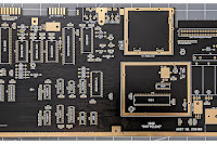
For completeness, here is a fully annotated diagram illustrating every component:
ANNOTATED DIAGRAM
 |
| Click for a larger image |
ANTENNA
And what about the missing Wi-Fi antenna? Well, in the pictures above you can see the empty U.FL/IPEX connector, it's the little round socket at the top right of the ESP32. We need to plug an antenna in there, and it just so happens you can get flexible adhesive Wi-Fi antennas that seem made for the job, like this one:
 |
| 2.4GHz Flexible Wi-Fi/BLE Antenna (U.FL) |
I have read that it is dangerous to the ESP32 to power it up without an antenna attached, so it's imperative I have this available from first use. The danger arises from a phenomenon called Impedance Mismatch and the resulting Voltage Standing Wave Ratio (VSWR); you will want to Google those terms to find out more but the result of not attaching an antenna is to risk burning up the ESP32, and we don't want that. The antenna I've selected has 3M adhesive on one side, and it's plenty small enough to stick in the bottom shell of the "Stumpy" cartridge case then bring the wire up and over to connect to the U.FL/IPEX socket. How this performs compared to an onboard antenna of course, remains to be seen.
UART CONNECTION
The next thing on the to-do list was to find a sensible way to connect the USB to UART module to the UART pads on my PCB. Luckily, some big-brains are way ahead of me here and the solution is this garish, fever-dream, day-glo "Pogo-Pin Probe Clip" (seriously guys, you run out of black filament?):
 |
| Pogo Pin Probe Clip - 4 Pins |
The pogo-pins on this comedy-colored clip are 2.54mm apart which is the same pitch as the pads on my PCB (it's almost like I planned this) and one simply connects some Dupont wires from the USB to UART module to the head of the pogo-pins and literally clamp this onto the pads, which should make a nice reliable connection without requiring extra hardware on my PCB, saving lots of valuable space.
That's all very well but up till now, this is all theoretical. I believe my design is sound and I've checked my connections against the original more times than I care to mention but there's only one way to be sure, and that's to make it a reality.
The crucial elements to having a PCB assembled are to make sure that every single component on the PCB is properly annotated with its designator, value, description, manufacturer name, manufacturer part number, distributor, distributor part number, package/footprint and any crucial build notes (such as polarity of tantalum capacitors etc). This takes a while, even for the handful of components on this build but at the end of the day this will generate a comprehensive Bill of Materials (BOM) which is essential to ensuring the parts you want to be used, will be used, and avoids any confusion.
The last thing I did was place a Drill Origin in the bottom left corner of the PCB edge cut to be used as a reference point from which to offset the location of all the components and drill holes for the automatic pick and place machines. That's it for the hardware (except a hefty bill).
SOFTWARE
As mentioned above, we need the program which will run on the ESP32. Such software is called a "sketch" (why? No idea), that's the C64_Chat_3_85.ino file I referenced earlier. We need a way to install that onto the ESP32 so I need the Arduino IDE software and once that's installed on my PC I need to update a bunch of libraries so the IDE has everything it needs to successfully program my ESP32.
We also need to program the EEPROM which will reside on the board, and that needs the correct ".bin" file. I'm using an 8K 28C64B EEPROM and at the time of writing the 8k bin file I needed was here.
All of this is detailed on the GitHub page and the Chat64.nl site but, unfortunately, the info gleaned from both is somewhat different. The Chat64.nl site appears to be out-of-date and so software version numbers and Arduino IDE library files to install don't correlate. The GitHub pages aren't the best organised I've ever seen either so finding everything was way more of a chore than it should have been. However, we got there. The links above are valid at time of writing but if things are ever tidied up, they may change.
PCB FABRICATION AND ASSEMBLY
I decided to use PCBWay for the build. This process needs to be done in two steps: firstly, the bare PCB needs to be fabricated. It's a four layer board and I'm selecting black soldermask (this is the way), white silkscreen and ENIG for the contacts. The edge of the PCB will be bevelled at a 30° angle. We're looking at a cost of about 50 USD for this step and a total of 5 boards (the minimum you can order).
The second step is assembly. For this, along with the Gerbers, we need to have uploaded a Bill of Materials and a component positioning file (these are generated automatically in KiCad with the PCBWay plugin). PCBWay will then track down all the components you've specified in the BOM (they appear to have links to Digikey and Mouser for this) and once they arrive, assembly begins. The cost for both PCB fabrication and assembly comes to about about 150 USD for all 5 boards. Then add shipping and total cost to me is about 180 USD, giving an initial Unit Cost of 36 USD (27.13 GBP). Prices fluctuate of course so this is just what I paid, at this time.
Building and Shipping took a moment. I uploaded my files on the morning of 29th November. The PCB was approved in minutes, but it wasn't until the morning of 1st December that the Assembly was approved. In that time someone at PCBWay audited my Bill of Materials, costed everything up and looked at lead times (i.e. the time taken to have parts delivered from stockist to them). As it turned out, for this design most components had no lead time, so I assume PCBWay had these in stock, however 3 components had lead times of "7-10 working days" so whilst PCB fabrication was completed on December 4th, it wasn't until December 9th that assembly begun and that wasn't finished until December 15th. Patience is very much key. All in, it took 18 days from initial order to eventually taking delivery on 17th December.
There was a nice big gotcha that's worth noting too. It transpires that one of the logic chips on the original PCB (the SN74LS244) is described in the original KiCad design file I downloaded as the Texas Instruments SN74LS244NSR. This is an error. The NSR suffix means it is the narrow body version of the chip. The footprint on the original PCB (and on my redesign) is for the wide body version of the chip (so the SN74LS244DWR). I confess to:
A: not knowing there were wide and narrow versions of this chip and so.
B: not noticing this discrepancy in my redesign and,
C: assuming the KiCad files would be correct.
This gaff was only spotted by the engineer during assembly. Ignorance on my part is no excuse however, I should have checked all that stuff so that's on me. Luckily, the narrow body version of the chip can be soldered to my board, by the skin of its teeth, so I got away with it, this time. It's not likely I'll ever order up more of these so it's moot, but I have updated KiCad for my design and my BOM with the correct chip; however, the original SMD KiCad files on the Chat64 Github may very well still be wrong. I am not registered with Github, nor do I have any intention of ever getting registered with Github, so I cannot raise an action to request a fix.
There was one other Engineer question concerning polarity and orientation of the LEDs but this was already noted in my BOM and would have been answered had the Engineer read the BOM fully. I guess these additional questions held things up for a few hours but I've no complaints about the service. For it to take just 18 days, total, to have a PCB manufactured from scratch and put into my hands will never cease to amaze me.
I already had the required EEPROM (5.67 USD) and Socket (2.77 GBP) and this I soldered to the PCB myself. Plus we needed the external antenna (6.55 GBP) and Stumpy cartridge case (5.95 GBP) so the cost of those parts must be added to the unit cost which comes in at a grand total of 46.78 GBP, shipped (that's 62.43 USD at today's exchange rate). Nobody ever said prototyping PCBs was cheap, however comparing this with the price of one complete SMD Chat64 from the official Etsy Store (43.88 plus 13.16 shipping = 57.04 GBP) and this becomes much more acceptable. Of course there's my additional one-off outlay for the USB to UART module (6.50 GBP), and the Pogo-Pin Probe Clip (5.50 GBP) to account for. Considering, however, that this is a unit cost and the unavoidable actual cost is 5 times that and I'm pretty safe in assuming nobody else will ever want to obtain this. Besides, this is very much a prototype so I won't be creating a shared project on PCBWay or providing Gerbers and BOM here.
TESTING THE BOARD
 |
| My redesigned Chat64 |
 |
| Close up of ESP32 and Antenna Connection |
 |
| Close up of 3.3V Regulator, UART pads and momentary buttons |
 |
| My completed cartridge and bespoke label |
When my redesign worked, first time, with everything going exactly as planned and as outlined above, you could have knocked me over with a feather. My ghast was utterly flabbered. I was pretty sure I'd thought it all through but this was all quite convoluted (for me) and there was always the nagging thought I'd screwed something up. As it was, I hadn't. Every planned step just worked from programming the ESP32 to the dinky flexible, adhesive Wi-Fi antenna. I'll be riding that high for quite a while. Had any difficulties arisen at all I would have outlined them here, but they assuredly did not.
After following the online User Manual, and getting my Wi-Fi credentials plumbed in, I used the MAC address and registered my cartridge. This prompted an email containing my unique registration code, and that needs entered into the account setup along with a username, After that, I was in.
When getting into the chat for the first time I was prompted to update the ESP32 and the ROM. This is a bit odd as it means both the ESP32 sketch and the ROM bin file on Github I had programmed in, mere minutes earlier, weren't the most up-to-date, and you really have to ask why? This, together with an unclear Github, the incorrect chip in KiCad, misaligned information between the web site and Github and (as I've just discovered) undocumented features of the chat room (e.g. scrolling) and it all feels a bit disorganised. Bart and Theo really need to take a moment, take stock, and get everything ship-shape. However, that gripe aside, this automatic update went perfectly, the cartridge reset itself and after some flashing on the screen, eventually booted back up. That's really very clever.
I then found myself in the chat, and was immediately being chatted to by a couple of users there. This took me quite by surprise as any time I've looked at the "who's online" page on the chat64.nl site, there's never been anyone online. I hadn't even read up on how to navigate the chat yet! That's not difficult incidentally but I did have to take a moment to educate myself. Anyway, we're moving into review territory here which is not the point or my purpose.
The point, and the purpose is to say, mission accomplished. I've used my cartridge for several hours now and there have been no dramas or issues at all. I've not yet missed having that reset switch either so no regrets.
The only question I have left, is how the wireless antenna is performing: all I can say with certainty is "it works". There's nothing in the existing software to measure the dBm (decibel-milliwatts). From the brief research I've done this would appear to be reasonably trivial for someone with coding experience to accomplish and it strikes me it wouldn't be impossible to add something to the Chat64 software. However, that someone is not me. What I may be able to do however is use one of my spare PCBs (remember, I bought 5 and I'll only be using 2), and write a short sketch to load into that and display the Wi-Fi strength (in dBm) to the Serial Plotter in the Arduino IDE software. If the mood takes me, this is something I may do in the future and if that transpires, I'll update this page accordingly.
Finally, I'm going to spend some time over the festive break looking into creating my own Chat64 server on a Raspberry Pi. If that works out, expect a blog chatting all about it sometime in 2026.
SCREENSHOTS
Captured via HDMI with my 250466 SixtyClone with HD64:
 |
| Chat64 Splash Screen (press any key to exit) |
 |
| Chat64 Main Chat (blurred for privacy) - Press F5 to toggle to Private Chat |
 |
| Chat 64 Private Chat (blurred for privacy). Press F5 to return to Main Chat |
 |
| Main Chat showing Scrolling Function (press CTRL + u or C= + u to activate) |
 |
| Chat64 Main Menu (press F1 from Main Chat to get here) |
 |
| Chat64 Wifi Setup (blurred for privacy) |
 |
| Chat64 Account Setup (blurred for privacy) |
 |
| Chat64 User List (online users in green) |
 |
| Chat64 Server Setup (if using own server, enter it here) |
 |
| Chat64 Help |
 |
| Chat64 About |
 |
| Chat64 Output Setup |