PART 5 – STARTING THE BUILD
In Phase 1, I outlined all the major components, where I bought them, and ran up a bill that certainly raised my eyebrow. In this phase I start to solder all of these components into a working machine, eventually. There is a lot to be said about how I got there and all is not plain sailing.
The site where I purchased the PCB contains a link to a Bill of Materials (BoM) which itself provided links to several online suppliers who can supply many of the required parts. This is very useful if sourcing your own components but note that many parts are hard to come by and available only on backorder with very long lead times. Do pay very strict attention to the components you've been linked to, to ensure suitability: whilst the values of the component may be correct, the pitch (the distance between the centres of the pins) may not be so be doubly careful.
For your reference and to help in identifying parts, I have written, and include below, an illustrated guide of all the internal components required to complete the build (minus the PCB and ICs) and for convenience, this includes a copy of the original list of parts for the 250466 from the C64/C64C Service manual.
The kit of PCB components I bought also came with a BoM which listed the parts included and their location on the board. This is extremely helpful. You must however take the time to methodically go through each component against the BoM to ensure everything is present and correct.
A magnifying glass is extremely helpful here to ensure you are accurately determining, for example, resistor band colours. As you can perhaps see from the above picture I segregated all components according to their reference on the PCB and made a note of the component values too. This is not a job to rush! Once separated and annotated I put all components into their own individual bags which kept them safe and separate until soldering time.
The C64/C64C Service Manual contains parts lists, schematics and board layouts for several PCB revisions, including the 250466 I'm building, though it must be said the readability of the service manuals available online is pretty poor. For that reason I have redrawn the board layout for the 250466 (click for a full sized image 6288 x 3090 pixels) which is labelled with the location of each part.
A copy of this layout is also included in the 250466 Illustrated Component Guide (link above). If you prefer a more interactive component locator, Eduardo Arana has created a magnificent page, linked
here, which allows you to select a particular component from a drop down menu and the resulting location is clearly highlighted on a graphic of the board.
I have also redrawn the 250466 schematics, again because scans available elsewhere are of very poor quality. Click for full sized images (6932 x 4516 pixels which can be printed very large should you desire):
1 of 2:
2 of 2:

IMPORTANT NOTE ABOUT LOGIC ICs
It is imperative, when sourcing your Logic ICs, that you obtain them from a reputable supplier. The market is awash with fake chips so the best advice is to stick with a dealer you trust.
Additionally, make sure that all the logic ICs you source are from either the 74LS or 74HCT families. For a project like this you never want to use: 74AHC; 74HC; 74AHCT; 74AC or 74ACT because they are either too fast or have the wrong threshold logic level.
With all parts finally present and correct, it is finally time to heat the soldering iron and make a start. I'm no expert but I know the principle of a good solder joint and though this took me a while (I really took my time) by spending a couple of hours a night I had completed the entire build within a week. To someone with more experience, I suspect this could be done in an afternoon.
This is not a soldering tutorial so anyone looking for one should look elsewhere, however, as far as the order in which to solder parts is concerned, I simply did what I've seen everyone else doing and started with the smallest, lowest components: resistors and ceramic axial capacitors and literally built up from there with the final elements being the port connectors and large electrolytic caps.
Whilst soldering, there was nothing which caused any problems and this appears to be a relatively simple build, well within the capabilities of someone who has a reasonable grasp of soldering techniques. My own problems began after the soldering, and after the first smoke test (which went perfectly: all voltages, in all locations present and correct) and after populating with all the ICs.
PART 6 - ARE YOU F*****G KIDDING ME!!!
It was a very excited and nervous me who flicked the power switch on the fully populated board for this first time to be greeted with...
Well, it wasn't the happy, familiar, "Ready" prompt that's for sure.
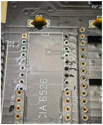
While I was populating the sockets with their ICs I was more than a little concerned to find that some of the chips went into the sockets a little too easily. I expected to have to give a very firm press to push them home, but for all but two (and only two which clicked firmly into place), the others just sort of slid in with very, very gentle persuasion. One I could lift in and out with my fingers quite easily. This alarmed me, and for good reason as it would turn out but at this stage I was committed so persevered.
When powering on for the first time I was presented with a blue screen, no border, and no text.
This was obviously disappointing but, in a perverse way, encouraging: the video signal was clearly working, which meant that whatever was wrong was probably straightforward. And given I was already unhappy with the sockets, that's what I honed in on. I figured something wasn't making good contact and so I simply switched off and re-seated every chip.
The second time I powered on...
Result!!!
But yeah, my triumph was short lived. The blue screen problem was cured but a whole new issue cropped up:
I left it on for a while to see how hot the chips got - to test this I was just grazing them with my finger. The very act of grazing the chips - not even pressing them - but grazing, caused the screen to fill with garbage characters then the computer to crash. This happened when touching the CPU, VIC and the ROM chips. I discovered through trial and error that taking the motherboard off the silicon soldering matt and putting it directly on the desk surface cured this but now when I touched ground, i.e. the piece of gold contact running right around the edge of the board this made the blue text on screen turn white - when I remove my finger it returned to normal. Weird right? Obviously an electrical issue but where the hell to start?
Again, my first thoughts were it was those goddam piece of crap sockets so I powered everything off, disconnected from power and used my multimeter between the solder joint on every socket pin on the rear of the board, and the leg of every IC, just to check that everything passed a continuity test. And guess what I found? A pin on the VIC chip was failing the continuity test. Stupidly I don't seem to have taken a note of which pin which is extremely aggravating now as I write this.
I should state at this stage that prior to all my diagnosing on the new board, I had tested the VIC-II, CIAs, ROMs and PLA in my original breadbin and they were working absolutely fine. This definitely helped in the process and gave me much more confidence that it was the sockets that were the issue here.
Re-seating the VIC cured the problem temporarily but it always crept back. I think as the VIC chip warmed up it was expanding just a fraction but enough to cause the leg of the chip to make a bad connection in the socket. Believe it or not I fixed it once-and-for-all by bending the leg of the VIC chip at a slight angle off vertical so that it could still fit the socket but obviously somehow made a good connection. Good grief.
Things came to a head when I ran my diagnostic cartridge. This showed that the TOD clock on one of the CIA chips wasn't working, and once again, bending the pins on the chip just slightly, fixed it. Bare in mind these sockets are tiny and I was bending the legs by minute amounts but this was clearly a WTF moment - who's ever heard of this shit? This should not be an issue!
That solved that problem but by now I was really pissed. I had spent a lot of cash getting things to this stage and I felt conned into taking delivery of unknown, unbranded sockets which were plainly just junk. As I stated in Phase 1, I emailed the supplier expressing my disappointment with their sockets. Part of their reply (which I found to be defensive rather than particularly helpful):
"These sockets come from a well established electronics distributor here in [REDACTED], so if there’s anything wrong I will definitely need to take that up with them, as these sockets aren’t particularly cheap. You are the first one to report an issue with them"
Now I can't legitimately throw around accusations. I have not a shred of proof, but I just simply do not believe, given how appalling these sockets were, that I am simply the unfortunate recipient of a lone bad batch. Not a chance. It is however, I concede, perfectly possible that no one has reported a problem and so I do take the supplier at their word. Personally, I'm never again sourcing a component I can't easily replace if I don't know its brand. Caveat emptor. And this particular emptor is now caveated to the max. I was particularly disappointed by the defensive and unapologetic nature of the replies received when I reached out to this company and will certainly never buy another kit again.
That aside, ultimately, whining and moaning solves nothing. I was left with a socketed board I couldn't trust. Yes it worked now, but how was I to know when the next failure would occur? Would simply moving it around knock something out of place causing yet another connection problem?
And this, ladies and gentlemen, is where I screwed up. Badly.
I've desoldered stuff before. I successfully removed the RF modulator and power switch in my original breadbin with no drama, I was pretty certain I could remove all these useless sockets right? Right? All it took was patience and perseverance. Easy right? Oh I was so badly wrong...
Looking at that picture, even now, makes me want to weep. What a mess.
See the problem here was a classic case of over-confidence, combined with appalling technique and, in the end, blind, to-hell-with-this-shit, fury.
My board was screwed and all I could see were pound signs £££ flashing before my eyes.
And here, on this cliff-hanger, we end Phase 2: in a state of despair; not knowing quite how to bounce back from a catastrophe wholly of my own making.
In
Phase 3 find out if I throw the whole lot in the garbage or if I somehow recover both my pride, and my computer.
(Spoiler: it's both).