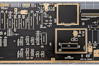
One evening, not so long ago, I was staring into the guts of my newly built SixtyClone Commodore 64 having a good think.
Truth be known, I almost get as much entertainment from simply staring at the innards of the machine I built as I do from playing games or coding on it, which means, the whole reason I embarked on this journey was a complete success. But there was still something niggling at me. That niggle goes a bit like this:
Someone else designed the SixtyClone board, I simply added the components I sourced from a Bill of Materials and soldered them in. Wouldn't it be something, wouldn't it be an even better feeling, if I could build something from scratch, that was all mine?
And this got me thinking. And that was why, one evening, not so long ago, I was staring into the guts of my SixtyClone mulling this over.
It occurred to me that this might not be completely impossible and indeed, it might be a very interesting experiment to attempt to build my own RF Modulator replacement just to see what happens. I specifically chose this over something else as there are enough components to make it a challenge, but not so many I would be overwhelmed.
I should say at this stage (and this will be painfully clear as we progress) I have only a rudimentary knowledge of electronics, not a jot of professional experience or training, and have never, ever, done anything of this nature before, so this is quite the leap (building a SixtyClone is a bit like painting by numbers and nothing like designing a whole new PCB from scratch). All I have available to me are the original schematics in the Service Manual and Google. To all of you reading this, for the love of all that is holy, please do NOT consider this as any sort of tutorial. I am, quite literally, guessing all of this. This is meant to entertain as you read about me slipping on metaphorical banana skins.
I'm well aware that many others have developed perfectly good RF Modulator replacements but it's my intention here to completely ignore all of these and to see just what I can come up with on my own. I will gain nothing by simply copying someone else's design, I would learn nothing, and I would consider this to be cheating.
So the personal challenge is set. As with all of my hair-brained schemes I like to break things down into bite sized chunks so here is a digestible list of what I will have to do to pull this off:
- Get to grips with the original schematics and decide which parts I do, and do not, need.
- Draw up a new schematic, with only the required parts.
- Identify and Source components.
- Build the whole thing on a breadboard to test.
Only if the above list is successful will I move on to Phase 2:
- Decide which design software I want to use.
- Learn how to use the software.
- Design the PCB in the software.
- Have the PCB printed.
Simple eh? In all seriousness, I rate my chances of building a working modulator replacement as zero, but let's bash on regardless and see how far I get.
Phase 1 - Part 1
Getting to Grips with Original Schematics.

The second is on Page 31, "MODULATOR SCHEMATIC #251696"
My SixtyClone is based on the 250466 PCB and if I look at the parts list for this in the service manual on Page 35 it states that the modulator to be used is #251696. I have taken the time to redraw this schematic and this is pictured above. This then is our starting point.
Now as schematics go, this isn't the most complicated thing I have ever seen, but that's not to say I fully understand it! With that said, it seems fairly obvious to me that we can break this down into chunks to make this a bit easier to digest, so lets do that.
First things first, what do the symbols on the schematic mean? If we don't know that then we're falling at the first hurdle. Luckily, for the most part, I do know this from building the SixtyClone and other wee projects over the years so lets go through them with the simplest explanations humanly possible:
 |
CAPACITOR A capacitor stores electrical energy. I assume this symbol to mean a Ceramic Capacitor. When a capacitor is connected to a power supply, its voltage gradually increases and its current gradually decreases. If disconnected from a power supply, the capacitor will temporarily maintain voltage. Note how this differs from the Inductor. In schematics these are numbered and always prefixed with a C. |
|---|---|
 |
ELECTROLYTIC CAPACITOR As with a Ceramic Capacitor this simply stores electrical energy but is capable of holding a greater charge and is polarized. In schematics these are numbered and always prefixed with a C. |
 |
DIODE A diode simply allows current to pass in one direction. The shape of the arrow in the symbol illustrates which direction that is. This is called forward bias. In schematics these are numbered and always prefixed with a D. |
 |
ZENER DIODE This differs from a normal Diode in that current can also pass in the other direction, this is called reverse bias. These are normally used for regulating voltage. In schematics these are numbered and always prefixed with a D. |
 |
INDUCTOR An Inductor stores energy in a magnetic coil of copper wire. When an Inductor is connected to a power supply, its current gradually increases and its voltage gradually decreases. If disconnected from a power supply, the inductor will temporarily maintain current. Note how this differs from the Capacitor. In schematics these are numbered and always prefixed with an L. |
 |
RESISTOR Like the name suggests, a Resistor will "resist" some current and are normally used to reduce, or limit, the current in the circuit. In schematics these are numbered and always prefixed with an R. |
| TRANSISTOR A Transistor is used to amplify or switch electrical signals in a circuit. In schematics these are numbered and always prefixed with a Q. If we google the term "transistor symbol" we find very quickly that this is an NPN Transistor. I'll come back to that later. |


1. The Color Circuit:

2. The Luma/Comp Circuit

3. The RF Circuit
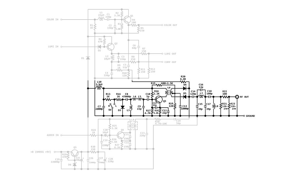
4. The Audio Circuit

5. The Power Circuit.