Prototyping with a Breadboard
Revision A
In Part 3 of this lunacy, I sourced what I thought were suitable components for constructing a new RF Modulator replacement. It is entirely possible that certain elements I chose, especially the transistors, diodes and inductors are not suitable but if problems arise we can address them later. I'm also going to repeat my mantra about this not being a tutorial. This is just an entertaining (hopefully!) narrative about trying to see an over-ambitious idea to fruition.
Just a few days after ordering, all the components had arrived and it was time to start my prototype. It seemed eminently sensible to build this in stages which would help to keep the complexity (for me) under control. I realise, as electronics projects go and based on our new schematic, this is actually very simple for anyone with good electronics knowledge but as previously stated, I have never done anything like this before so I will take all the reduced complexity I can get.
 |
| All components received |
I decided pretty much immediately that I would concentrate my first efforts on building the power circuit. This element has very few components and seems perfectly straightforward, but there was one tricky part to overcome first. Let's get into it.
This, if you recall, is schematic of the power circuit in our project. There are only 6 components here, not including the wires:
1 x Resistor
2 x Ceramic Capacitors
1 x Electrolytic Capacitor
1 x Zener Diode
1 x Transistor
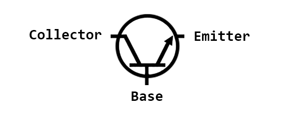
Everything here seems straightforward except the transistor. Lets look at this in isolation for a moment.
 |
| Schematic NPN Transistor Symbol |
I know from my Googling that a NPN transistor has 3 parts to it:
The Base
The Collector
The Emitter
I don't pretend to understand what these are in any technical way, but it is important to know where they are, because we must know how to wire it together correctly.
The diagram makes this easy. The bit with the arrow is always the Emitter. The bit in the middle is always the Base which means the remaining part must be the Collector. I can annotate the diagram accordingly:
Now, a simple picture like this is one thing, but applying these same labels to an actual transistor is a whole different ball game. In normal circumstances you would simply read the datasheet which would tell you exactly where the Base, Collector and Emitter were located. The particular transistor I am concerned about in the power circuit is the 2SC2120 which is manufactured by several different companies. The one I bought on Ebay did not specify which company made it, simply advising generic. This is not helpful. Especially when I tell you that the positions of Base, Collector and Emitter were different depending on who manufactured it. In short, I could not use a datasheet and had to find another way. After much Googling, here's how I resolved it. Time to dig out my much cheapness multimeter:
1. Insert Transistor into a breadboard (we'll talk about breadboards a little later) for stability and give each pin a number:
2. Set multimeter to diode test setting:
3. Undertake each of following steps in the order shown:
- Apply black probe to pin 1 and red probe to pin 2 and record reading.
- Apply black probe to pin 1 and red probe to pin 3 and record reading.
- Apply red probe to pin 1 and black probe to pin 2 and record reading.
- Apply red probe to pin 1 and black probe to pin 3 and record reading.
- Apply red probe to pin 2 and black probe to pin 3 and record reading.
- Apply black probe to pin 2 and red probe to pin 3 and record reading.
4. Compare results. These were as follows (where my multimeter displayed a "1" this means that the circuit is open and no current is flowing):
- 1 - open
- 1 - open
- .618 Ohms
- .620 Ohms
- 1 - open
- 1 - open
This was pretty definitive. Only steps 3 and 4 produced anything other than an open circuit:
 |
| Step 3 |
 |
| Step 4 |
In both these Steps the red probe of my multimeter was on Pin 1 and this tells me categorically that Pin 1 is my Base.
Between Pin 1 and 2 the resistance was .618 Ohms. Between Pins 1 and 3 the resistance was .620 Ohms. The Collector always has the lower resistance which means Pin 2 is the Collector. Pin 3 must then be the Emitter:
We will absolutely, definitely need to know this later. As I wrote earlier, I had no prior knowledge of this and had to Google everything to discover what you've just read. In the next step we'll find out just how successful all this Googling was.
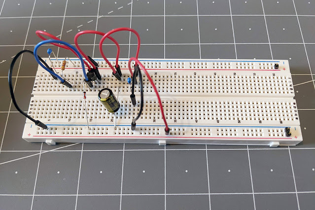
As I said above, I'm prototyping this on a breadboard, which, by design, is a very convenient way of laying out circuits for testing, in exactly the way I'm doing here.
The breadboard is very simple: there are two strips at the top, one marked "+" for a positive and "-" for a negative. These positive and negative strips are replicated at the bottom. Any power going through these strips will go the entire length of the board. The remaining holes are for our components. Holes on Row 1 marked "a, b, c, d, e" are all connected together, however they are NOT connected to holes "f, g, h, i, j". Nor are they connected to Row 2. The same applies to all other rows (Above picture is sideways so rows look like columns).
For initial testing, I'm going to be using a 9 volt battery to power the board. If you look back at the cropped schematic of the power circuit near the top of the page, you will see it states "+B (UNREG +9V)". Ignore the +B part, all I'm interested in is the UNREG +9V. More Googling tells me this means there are 9 volts unregulated, going into the board. What the hell does that mean?
Well, an unregulated power supply simply means "the obtained DC voltage does not remain constant due to the variations in load current, variations in mains voltage and changes in ambient temperature".
In other words, this 9 volts is liable to fluctuate. As I determined in Part 3, this part of the board I'm building is a Voltage Regulator, so I am simply regulating an unregulated voltage, i.e. I am making the voltage constant. A battery, Google tells me, is also unregulated, though I have no idea if the fluctuations in voltage a battery makes are comparable with the fluctuations in the C64, but it's a start, and it's easy. I will connect the battery to my breadboard as shown:
By doing this you can see that the red strip along the top will be my + Positive Voltage, and the black strip all along the bottom of my board will become the - Negative Voltage (which is replicating Ground - again, Google told me this).
The next part is to simply insert my components exactly as the schematic tells me, allowing for the limitations the breadboard imposes regarding connections:

- Ceramic Capacitor C29 has one lead inserted into the positive strip, then a wire will take the other lead to the negative strip.
- Resistor R29 has one lead inserted into the positive strip, a wire then connects the other lead to the base of our transistor Q5. Remember why I needed to establish which pins on the transistor were which? This is why.
- Zener Diode D6 has the cathode end (i.e. the end with the black line) placed at the base of the transistor Q5 and the other end connected to the negative strip.
- A wire connects the Positive Strip to the Collector of Transistor Q5.
- The Emitter of Transistor Q5 is then connected to the Positive side of Electrolytic Capacitor C25. The negative side of C25 is connected to the negative strip.
- The Positive side of Electrolytic Capacitor C25 is then connected to one lead of Ceramic Capacitor C26. The other lead of C26 is connected to the negative Strip.
- A final wire then connects to C26 and can be placed anywhere we need the Regulated Voltage. In the picture above I've connected it to the unused bottom + Positive strip but we can put this wherever we need it later.
I realise that may seem complex but when broken down into individual parts, it's quite straightforward. In theory. Now it's time to put the actual components into the breadboard. This is what it looks like:
Everything here is laid out pretty much exactly as I illustrated above and in this configuration, my regulated output (+) voltage will now be on the very bottom strip. On the right you can see I have added some pin headers: this is so I can connect these to my multimeter to take some voltage readings. I've spread the components out more than they need to be but this makes it easy for me to see what is were.
There is nothing else for it now but to connect the battery:
As you can see, by placing my multimeter red (+) probe on the pin header on the bottom strip, and the black (-) probe on the pin header in the negative strip, I can read the voltage now being output by my now regulated power circuit:
5.79 volts.
Let's think back to what I said in Part 3:
"It seems that calculating the Voltage Out in our circuit is a simple formula:
VOUT = VBE - VZ
To obtain the values for VZ and VBE I needed to consult the datasheets for the Zener Diode and Transistor I chose (1N4582A-1 and 2SC2120 respectively). If I am reading them correctly, then the VZ is 6.4V and the VBE is 0.5V (min) to 0.8V (max) which gives us a VOUT of between 5.6V to 5.9V."
As you can see, I estimated our output voltage to be between 5.6V and 5.9V.
My actual measured Output Voltage is 5.79V. only 0.04V from being exactly midway between my calculated range. Not too proud to admit I did allow myself something of a premature wry grin. This means I did, in fact, read the datasheets correctly, and I also determined the correct pins on the transistor. Queue more premature wry grins. Definitely premature: I know whats coming.
If I'm understanding the principle of this circuit, we can input any unregulated voltage (up to the max the components can take) and the voltage output should stay at 5.79V. Theoretically then, this circuit should be able to handle any variance between the unregulated 9V in the actual C64, and that from battery I'm using here. I think.
So, our unregulated 9V is now being regulated down to 5.79V. Not being able to spot anything wrong, I thought a good wee test right about now would be to see if I could now get this to power an LED. I have an electronics "fun" kit full of them and it's a very simple job to connect one up, along with a resistor, to see what happens. Remember, I now know my Voltage is where it should be (pretty much exactly) but I've no idea about amps or watts, so I figured this would serve as a simple smoke test too (i.e. would I blow them).
As you can see, I simply moved my Voltage Out wire to a different place on the board, connected a resistor (in this case a 1K Ohm 1/4 watt), connected the positive (long) leg of the diode to that, and the other (short) leg of the diode to negative.
No smoke, no drama, it just worked and after leaving this on for a few hours nothing got hot, not even warm. That was encouraging. I figured I had a working power circuit I could use to power the rest of the board. Of course I'm not counting my chickens, plenty can still go wrong and even though this appears to have been a total success, because I'm still ignorant of amps and watts there is every possibility I have too little, or perhaps too much power to get this to work.
I replicated this effort with both the Color (More often called Chroma) and Luma/Comp (Short for Luminosity and Composite) circuits, creating each on their own breadboard:
 |
| Chroma Circuit |
 |
| Luma/Comp Circuit |
Then I clipped all three breadboards together, made sure power was going to all boards, and ground was going to all boards, and any interconnects between boards to give me one complete circuit:
I then labelled all of my input and output wires so I would not forget what they were later.
It was then time to actually test what I'd built. I fretted about this for a good few hours before actually plugging it in to my C64: I was extremely anxious about having messed something up and feeding a bunch of errant volts back into the main PCB. But I eventually found my nerve and went for it.
When I built my SixtyClone I wanted to be able to easily add and remove any modulator replacements I obtained so I inserted 8 pin headers:
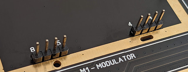 |
| Modulator Pin headers. Notice the numbers on the board. |
I have used socketed jumper wires for my inputs and outputs. These socketed jumpers fit snuggly onto the pins on the board:
All I needed to do was not mess up the order so I threw together a quick graphic from info in the Service Manual that I used as a reference, with each pin labelled in the same way as I was viewing the board:
NB. On some Commodore 64 PCBs, Pin 8 is NOT connected to ground. I believe this has to do with the configuration of Jumper J1 on the motherboard (the G.PAL / I.PAL jumper). I properly ensured that in my SixtyClone Pin 8 was indeed connected to ground.
I made these connections and warily powered the C64 and TV on. Impressively, I didn't get nothing. But I didn't get a proper picture either. Full disclosure: I was too preoccupied with checking my connections and touching the transistors to check for heat that I didn't take a picture of the screen but I have made a graphic of what I saw and it basically looked like this:
Thin angled lines scrolling down a back screen.
I powered everything off and had a think. I seemed to remember that the diode at D1 could be removed though in retrospect, and because I cannot find any source for that assertion with this type of regulator, I guess I made it up. Anyway, I removed that diode from the board thinking it would change the power behaviour to the Luma and Chroma, rewired the connection and powered back on to see what, if anything, would happen.
This time I actually got a recognisable picture, but it was a terrible blurry mess. I could however see enough to recognise that characters were appearing on the screen as I typed. Here's another graphic approximating what I saw:
It was right then, about 20 seconds after powering on without the diode D1 that I smelt the familiar tang of burning electronics and I switched the power off immediately. Woops!
Finger probing I felt immediately that the transistors were all burning hot but subsequent testing with the multimeter showed they were still working. What wasn't working, however, was the Zener Diode which was toast. RIP.
Obviously I tested my C64 after this and it was fine so no damage done there but my initial build, not unexpectedly, was problematic so it was, quite literally, back to the drawing board.
I cannot be 100% sure about what's happened here. If I had left things running for a bit longer without removing diode D1 would it still have burned up? Or, was it really removing diode D1 which killed it?
Google tells me a diode (not a Zener, but a regular diode) simply allows current to travel in one direction. Like a valve I guess. By removing it, I have allowed current to travel in both directions. Was it this that killed my board?
Or, was it simply that my 5.79 volts regulated output is way too high and that's what burned everything up?
Was it both? Or something else?
After a great deal of deliberation, here's what I think I've done wrong: I have mixed components derived from two different modulator schematics without fully implementing either one. My power circuit components were derived partially from schematic #251025, but I used the layout of circuit from #251696 because I had assumed the parts were interchangeable. But if I look at #251025 in the Service Manual I have not implemented everything it specifies. Although it's very hard to make out what the component values should be, I know everything highlighted here is either different, or missing, from what I built and this must affect the outcome:
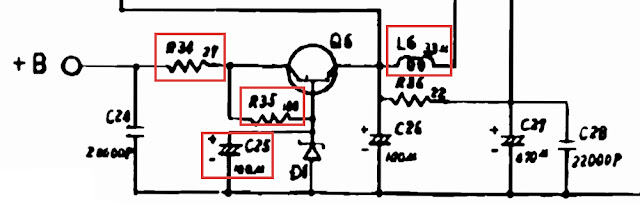 |
| Power Circuit Extract from Schematic #251025 |
Another thing. After much thought it dawned on me that the last C64's Commodore made, have a different voltage going into the modulator. Not +9 volts but simply +5 volts. Now in all other respects these newer models should be doing the same thing in the modulator to get the video signal to the TV so I now have to assume my voltage of 5.79 Volts (and who knows how many amps it was pulling!) was just too high.
The evidence is quite clear: my circuit WAS outputting a signal (it even managed a color one, albeit briefly), but it was corrupt and because everything started getting toasty, and my Zener was killed, I'm going to assume it's coz I bolloxed up my power circuit. I think I need to admit to myself that I'm not going to be able to replicate this particular type of power circuit because even if I understand the principle, I still don't really get it it, I can't clearly make out the necessary values and I can't get all the exact components.
So. I am going to completely scrap my existing power circuit and build something simpler.
I know, from building the SixtyClone, that there are single component Voltage Regulators - one of which, the 7805, outputs 5 volts. I also know from lots of Googling, that Voltage Regulators come in all shapes and sizes. In fact, if I search for "5v Voltage Regulator" on the very first page of image search results, there is something that looks like a transistor:
Following this up I discovered this was a DL7805 5 volt regulator. And this would be absolutely perfect as I wouldn't need to change my schematic all that much to implement something like this. A quick visit to Digikey revealed that particular part was unknown to them but simply searching for 5v regulators in a TO-92 package (which is the same package, or style, as my transistors hence they look the same) I found the L78L05ACZ-AP.
If all I want is a steady +5V fixed output which can handle a +9V unregulated input then the datasheet tells me this, plus a couple of ceramic capacitors, in the following configuration should do the job:
 |
| Extract from L78L05ACZ-AP datasheet |
With this there are no Zener, resistor or transistor values to worry about. All in all a much simpler design.
While researching the purpose of the capacitors in this datasheet (referred to as
decoupling capacitors, Wikipedia tells me "
Noise caused by other circuit elements is shunted through the capacitor, reducing the effect it has on the rest of the circuit"), I also found an interesting
Q&A on StackExchange which mentions adding some 10μF electrolytic capacitors to this design for "ripple smoothing". Ripple apparently = bad, so I will add them to my shopping list for experimentation.
And with that, and some renewed enthusiasm, I embarked on Revision B of my build which I will talk about in the
next entry.