Building the Schematic in KiCad
If you've been following along with this series of posts about trying to build an RF Modulator replacement from scratch, you'll know how I got to where I am now. There have been frustrations, confusion, misunderstandings, blind alleys and a memorial service for a Zener Diode. Ultimately though I achieved something approaching a staggering triumph. Some might call it blind luck. Either way, at the end of Phase 1, I had a working prototype which I've dubbed the "Janky as F**k 64" , or JAF64 for short.
 |
| The JAF64 |
Here, at the start of Phase 2, I need to take the design and replicate it in software. The software I selected for this task was KiCad.
It must be said, I cannot possibly give a blow by blow account of everything I had to learn and what you need to know to start designing a PCB. Seriously. This series would never end! And we do need this series to end at somepoint.
So with that said, what follows is a heavily abbreviated summary of my experience with KiCad.
On first opening the software (I'm using V6.0) you will be presented with the following interface:

KiCad is a suite of individual elements that work together to help bring your project to completion. The first thing you need to do is create a new project. In the screenshot above I've created a project called "Example" and it has automatically created two files: "Example.kicad_pcb" and "Example.kicad_sch". These are the two elements you will be using 99% of the time.
In the "...kicad_sch", the Schematics Editor, it will come as no surprise that you need to construct your schematic, and once that's complete, you use the "...kicad_pcb" the PCB Editor, to import all the parts and connections you specified in the schematic, to construct a virtual PCB.
So, the first thing that needs to be done is to start building the schematic. Simply double click the "...kicad_sch" element and a blank schematic will open:

This is the blank canvas on which the schematic needs to be drawn. There are a bunch of menu options and icons which can seem pretty overwhelming at first but most of the time I found myself only really using a couple. Most importantly, you need to be able to place components. To do this you need to find "Add Symbol" in amongst the icons or menus:

I found myself accessing it through the "Place" menu most of the time but there is also an icon to the right which will do the same thing. As will pressing "A" on the keyboard. Either way, a new window will open:

This is where things get messy. You need to find the symbol for the component you need from amongst a list of over 17,000 symbols and it isn't particularly obvious. Say for example I know I want to insert a capacitor:

I narrow down my search by starting to type the word "capacitor" in the filter text box at the top of the window. After I had typed "capa" the available items had diminished somewhat and I can start to see item names like "D_Capacitance" and "C_small" and so on. If I'm looking for a symbol for a regular unpolarised ceramic capacitor, then at least one appropriate symbol is found by selecting the item "C", as pictured, C being the universal designation for a capacitor in a schematic I guess? With "C" selected, and the symbol that I want presented, I press OK.

This brings me back to my blank template where I can just use the pointer to drop the symbol wherever I want it. The next thing that must be done is to give this capacitor a unique reference number, and we must tell the software the value of the capacitor (i.e. it's capacitance). You can't omit this or KiCad throws a hissy fit later.
By right clicking anywhere on the symbol, a menu will appear:

From the menu, select "Properties..." as shown.

The Properties window will open. Beside "Reference" type the unique reference you want to give your symbol (in this case I used "C1") and beside "Value" enter the capacitor value, which in this case I've entered "4.7μF". Then press OK.

The symbol is now labelled. If I want to rotate the symbol, I simply press "R" and it will rotate 90 degrees:

The final thing that MUST be done with this symbol is to assign a footprint. This is an absolute pain in the arse but there's no getting away from it, KiCad needs to know the physical dimensions of the part so we know how much space it will take up on the PCB afterall.

Once again, right click on the symbol and this time select "Edit Footprint" (or press "F"). A new window will open:

If there is already a footprint assigned to the symbol, you will see a designation entered beside "Footprint", but in this case it's blank so we need to find a suitable footprint in the library. Press the button that looks like 3 books to the right of the window and another window will open:

And once again we are required to search through a list of thousands of footprints to find something suitable:

Here, at the top left, I started to search for "capacitor" and the available options diminished. I know I want a "through hole" capacitor so the abbreviation for that is THT (as opposed to a surface mount capacitor which has an abbreviation of SMD for example). So I select Capacitor_THT on the left, and to the right of that I am then presented with a long list of available footprints for through hole capacitors of all varieties. Here it's simply a case of finding the most suitable footprint based on the type and dimensions of the capacitor in question. In this case I decided that the footprint for a ceramic disc capacitor with 5mm pitch (distance between component legs) would be the best so I selected that and a picture of the footprint appears in the main window. You will need the datasheets for every component handy so you have some idea of the footprint you need.
To assign the footprint to the symbol press the button that looks like a chip with a red upward pointing arrow (highlighted):


Press OK and you will be returned to your schematic. Nothing obvious will have changed but you have now done everything necessary to ensure that component will export correctly to the PCB building element.
You then need to repeat that whole process for every single element on your schematic. You will age drastically doing this, though in fairness all the capacitors I used in the end had the same footprint so I was able to simply copy and paste the initial symbol and only needed to change the reference and value. The same was true with the resistors.
Obviously you need to "wire" your components together and as well as being in the "Place" menu, you can access the Wire icon in the menu to the right:

Pressing this will allow you to click on a node of your component and start adding a wire to it:

Here in this simple example you can see I've added a wire to the right node of my capacitor and started drawing it to the right. And that's pretty much the jist of it. You add components, rotate and position them, apply unique references and values, add the appropriate footprint, wire them together and repeat over and over again until the job is done. It took me flippin hours to do my extremely modest schematic but we got there in the end with a lot of help from YouTube:
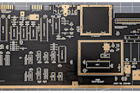
 |
| Click for a much larger image |
By far the most complicated part was working out how to correctly tell KiCad I was bringing the power and signals into the board from an external source and exporting those signal to an external source (that external source being the 250466 C64 PCB) but I did work it out eventually thanks to YouTube.
As I've said, I have summarised but the above is enough info to get anyone started and there are enough tutorials online to answer all questions that might crop up. That's how I got through it anyway and if I can do it, anyone can.
The final step before progressing to the PCB design is to perform an Electrical Rules Check. Press the button along the top of the screen that looks like a checklist with a red checkmark. This is really important to ensure you haven't messed up.

You are aiming to have no Errors and no warnings.
As I said, for me this took a long time to get right but I did eventually get there. In Phase 2 Part 2 we will import the components I specified in this schematic into the PCB designer and get the creative juices flowing.