Designing the PCB in KiCad
In Phase 2, Part 1, after much graft, I got the hang of designing my modulator replacement schematic in KiCad. Now I am ready to take all the parts I have specified in the schematic, and import them into KiCad's "PCB Editor" to begin to layout the actual printed circuit board (PCB) I want to have built.
This is both daunting, and exciting. Daunting because, as with pretty much everything I've done so far I'm still winging it. Exciting because this is the stage an actual working PCB might actually start to see the light of day.
I'll say right upfront what I found most difficult about laying out an actual PCB was moving my thinking away from the breadboard design. In retrospect I actually found laying out my prototype breadboard extremely easy as the physical limitations of a breadboard force you to create a logical "chain" of components. It was something of a struggle to apply some lateral thinking to what I was doing and modify the layout to favour a circuit board. However, this is my first ever attempt at doing anything like this and if I can produce something which works, I'll consider that a triumph. I can always worry about a better layout later.
Before diving into the software, I had a few initial thoughts from the outset that will determine how I progress.
Firstly, I knew that I wanted my PCB to utilise ALL of the available space on my SixtyClone board:
As you can plainly see, outlined in red there is a blank area on the SixtyClone PCB which is approximately 6cm x 6cm specifically for an RF Modulator. It made sense to use all of this available space. Nothing else is going here so why wouldn't I?
Secondly, I wanted to keep all of my different circuits (Chroma, Luma/Comp, Power) as physically far apart as I possibly could to prevent the signals from leaking into each other and introducing interference or cross-talk (defined as: undesirable signals from a neighbouring transmission circuit). With this in mind, I knew from the outset I wanted a 4 layer PCB. One layer would be used predominantly by the Power Circuit, one for Chroma, one for Luma/Comp and the fourth for Ground. In my brain this allows me to keep them all physically separate both vertically and horizontally, though I'm well aware that because energy and electromagnetic fields travel along the path of the circuit and are not actually in the copper per se that this is far more complicated than it seems and my thinking is probably naïve. This is all very "suck it and see" and there's a lot I simply don't understand. The big question I suppose is "do I understand enough to pull this off?" We're already well beyond anything I thought possible so let's bash on with guileless enthusiasm.
Ok. I know I want my PCB design to fit inside an approximately 6x6cm square. I also know that I must have 8 connection holes in the PCB to accept my 7 input and output signals (I'll also have a hole for the audio signal but that won't be connected to anything). I also know that these 8 holes will basically be a fixed reference point within my 6x6cm design. They need to be in a fixed position to allow connection to the SixtyClone board so they cannot move. I also know I can't simply have my PCB supported by the 8 power and signal pins alone, it's far too big for that, so I'm going to have to incorporate some means to physically support my PCB onto the SixtyClone AND I want it to be able remove the board so it can't be soldered directly to the SixtyClone. I have some ideas but first I need to get some more precise dimensions than my 6x6cm approximation. For that it's back to the Service Manual which, on Page 26, provides layout and dimensions for the RF Modulator:

This is a really bad scan (and, unfortunately, the only one I have) so the first thing I did was create a cleaner copy:
Now far be it from me to criticise anyone else, and this is probably just me being stupid, but I found this far more confusing than helpful. Let's break it down:
I can clearly see the 8 holes in the board, labelled 1 to 8 for my power and signal pins and I can also clearly see that the gap between pins 4 and 5 is 24mm. This is good and gives me the first dimension I need. If we then suppose that I want the middle of my board to be halfway between these, then the middle of my board is 12mm between them. So far so good - this would be the red vertical line in the above diagram. What this schematic doesn't give me is the outside dimensions of the original RF Modulator PCB. The 60.8mm measurement is between the pins of the metal shield surrounding the modulator PCB but we can easily surmise that the original modulator is within that.
For my board, I want to utilize two of the locations for these pins as locations for holes to support my board on the SixtyClone. My idea is to use 10mm M2 standoffs bolted to the existing holes on the SixtyClone so I want the exact positions of the circular hole at the bottom right of the above diagram and the circular hole at the bottom left (I'm not interested in the oval shaped holes) relative to the fixed position of the 8 input/output holes. Given the information available in this schematic I'm not entirely certain I can do that. At no stage is it explicitly stated that the middle horizontal line is in fact, in the middle - I have to assume it is. In the following diagram I've entered dimensions I can extrapolate; question marked those I can't without assumption; and in purple, measurements which when I extrapolate further make no sense and are contradictory:

Example: if, from the vertical centre line it is 12mm to the middle of connector 5 and connector 6 is another 2.5mm as specified in the original schematic, that means the distance from the centre line to the middle of connector 6 must be 14.5mm. It must then hold that the distance from the centre line to connector 3 must also be 14.5mm which means the total distance from middle of connector 3 to middle of connector 6 is 29mm. Now in the original schematic it's very hard to make out but I think it says 29.4 (possibly 28.4) neither of which make any sense and that's kind of crucial to know because I need the distance between holes "J" and "I" which could be 29mm or 29.4mm?
For clarity it's the holes I've labelled "F" and "I" in the above diagram I'm trying to precisely locate because these are where I want to mount my PCB. Maybe I've just had a failure of logic but I'm just not seeing how I can do that with the dimensions Commodore provided without making assumptions, other than hole "I" which I can extrapolate as 57.4 mm from connector hole 3 (but only if we assume the centre of "B" is in line with the centre of connector 6 which is also in line with the centre of "J"). What a mess. Or maybe I'm just getting hung up on 0.4mm difference which possibly isnt that big a deal. A good schematic shouldn't leave you guessing though.
Add to all that, the signal and power connectors I'll be using are 2.54mm apart and NOT the 2.5 indicated in the schematic, in the end I pretty much abandoned trying to get this to work and went with the brute force option of taking the actual RF Modulator I removed from my breadbin C64 and punching the pins through a "post-it" note and measuring the distance between them. I figured this was just easier and probably just as accurate.

I suppose we'll see if this was successful if I'm ever holding the PCB I'm designing in my hand!
Now that I know how I'm going to position the 8 input/output holes and the two holes for securing my PCB to the board, I can create a PCB outline in the PCB Editor with these elements as fixed locations and then build the rest of my circuits within these boundaries:
I won't pretend it didn't take me a while to work out how to do this relatively simple process (especially the curved corners), but by using the ruler tool and user layers to store temporary marks and annotations I was able to position these elements precisely where I think they need to be relative to each other. I hope it now obvious why I wanted to pin these measurements down as it's now perfectly clear the area within which I can build my circuits.
My design measures 63.6 x 64mm and is slightly off centre - a vertical line between the 8 holes is NOT the centre of the board - rather there is 33mm between the left edge of the board and this line, and 30.6mm between this line and the right edge of the board. This is to accommodate the metal cartridge guide which I will be inserting into my board at some point. I think I've accounted for all this correctly. We shall see I guess.
In the above image, I deliberately hid many elements to illustrate the initial setup. In reality, the first thing I did after setting up my board outline was import ALL my components from the Schematic Editor. This is done by pressing the button I've highlighted in red below:
Rather than demonstrate what happens if we do this with all my components which would just be a confusing jumble, allow me to demonstrate what happens if I just import the components for a simple 5v regulator (2 ceramic capacitors, 2 polarised electrolytic capacitors, the voltage regulator and the necessary pin connectors):
On import, KiCad just bunches all your components together and it's up to you to separate and order them. In the image above I've pulled them apart so that you can see the individual parts. You can clearly see there are "wires" connecting the components together and this is KiCad's way of telling you which components need to be connected to each other based on the schematic. The more components you import, the more confusing this "rats nest" of wires will become.
By moving, rotating and generally just being imaginative, below is one way in which to connect the components:
To illustrate my point I've very quickly thrown together an example of how you might arrange these components, and I've used the "route tracks" tool to literally draw my traces (in red) between the parts of the components that need to be connected. As you do this, the rats nest of KiCad's connection wires will disappear because it knows when you have connected components together. Obviously I'm definitely not saying this is the best design, it's just one way that seems both compact and meets all the design rules. For Ground you will see that there are no tracks or wires at all. This is because I've created a "filled zone" on a different layer which to all intents and purposes is just a solid layer of copper which links all the ground points together but leaves the other points alone:

In the above illustration the "filled" ground zone is now visible and looking closely you can see that the component holes which need to be connected to ground are connected to this zone by "spokes". Everything else is isolated from the zone and therefore free to go about its business.
Now clearly I've not covered every single step. Once again I have summarised the whole process massively but this is the general idea: You position your components in such a way as to ensure the traces are as short as possible, whilst still ensuring the electrical rules are followed. It's very much like a puzzle and you need to think logically and laterally to make this as successful as possible. I poured over all of this for days and days until I had a design I was reasonably happy with.
The PCB Editor in KiCad also allows you to see a 3D view of your board. This is extremely helpful in giving you an overview of your progress and I will admit I found using that very satisfying! For the quick example I threw together above the 3D view looks like this:
Obviously you can rotate this any way you like to get a view from any angle.
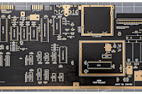
So with the quick example now explained, it was using these exact same principles that I finally managed to design a PCB for my modulator that I was reasonably happy with:
And there it is. My "JAF64" has finally been turned into a virtual PCB. It has my desired 4 layers, I believe the dimensions are as I need them to be and I've kept all of my circuits as far apart from each other as I can. Now this is not to say it's perfect, it's not, and I've already thought of ways I can change this for an improved Revision C. However, there comes a time when you need to draw a line in the sand and say, "Enough, let's get this thing manufactured and let's just see how it measures up." So that is exactly what I did.
If you've ever watched a YouTube video which has any connection to electronics or retro-computing almost all of them are sponsored by PCBWay. I'll be honest, I have no idea which PCB manufacturers are better than others but being that I knew about PCBWay from being subjected to a bombardment of advertising, and being that I could sort of understand what I needed to do to get this manufactured via their site and given that the initial quote was around what I thought was a fair price I just thought "to hell with it" and went with them.
A page on their site told me how to export Gerber files from KiCad which I did, then uploaded. I selected a 1.6mm thick board, with black solder mask, white silkscreen and an Immersion Gold finish which is what I think will closely match my SixtyClone board. The cost for the minimum order of 5 PCBs and postage to my home in Scotland was $88.82 USD. Total cost per board then is $17.76 (or $11.94 excluding postage). Below is a screengrab of the total progress of my order so you can see the timescales and steps involved: