Designing a C64 RF Modulator Replacement Phase 2, Part 3

If you've been following along then you will know that over the previous instalments I have taken you on the bumpy ride of designing and building a brand new RF Modulator replacement (The JAF64) for my 250466 SixtyClone board with no real clue what I'm doing, just to see if I could, and for the LOLs... though to be fair there has been far more cursing than LOLing.

Here, in Phase 2, Part 3 and the penultimate entry of this saga, I finally take delivery of the PCB design I have poured over for weeks. For clarity it was on the 2nd of May 2022 I first had the idea to do this, and the 20th June 2022 I received the manufactured PCBs. 50 days. In that time I've got to grips with the schematic, built a working prototype on a breadboard, learned the basics of using KiCad and managed to successfully submit Gerber files to have the PCB built. I'm certainly not unhappy with this timescale.


I spent the morning of 21st June 2022 soldering the components into the first PCB and learned several valuable lessons to take forward to a future Revision C:

  1. The solder pads were really very small making soldering something of a chore. I will be enlarging these in any future revision.
  2. The 3 solder pads of the Voltage Regulator and Transistors were awfully close together making soldering them without bridging anything a pain.
  3. The holes in the solder pads for the component legs could stand to be enlarged just a smidge to aid flow of solder through the board.

However, demanding as it was, I managed to solder it all together over a few hours without issue.

Me and my JAF64
Yeah, I get outside sometimes


And now, finally, I get to plug it in to my SixtyClone for the first time and turn it on:

Video Out - ignore the moiré - that's not present in actual output


I had a picture, but it was devoid of color. Monochrome. Achromatic. Black and white. Oh FFS.

Obviously, this meant my Chroma circuit wasn't working and I puzzled over this for hours.

  1. I double checked all my solder joints. The multimeter gave me correct continuity everywhere.
  2. I double checked my components to ensure I hadn't accidentally soldered the wrong components in the wrong places. Everything was correct.

This meant that it was nothing obvious. I started to wonder if maybe a component was faulty and so with the board plugged in to the SixtyClone and with everything powered up I started just poking at different parts on the Chroma circuit to see if anything changed on screen and believe it or not, eventually this paid off.

I had this idea to piggyback a resistor on to the resistors in the board, and by that I mean I just hand-held a known working resistor and touched the legs of that against the legs of the resistors in circuit, just to see if anything happened. When I got to R1, like magic, the screen lit up with sweet, sweet color.

Of course I assumed that R1 (a 1K resistor) was toast and I'd probably burned it up by overheating while soldering so I replaced it and tried again:


Same f*****g problem. What the hell? Once again I bridged it with a known working resistor and once again the color came back. WTF?

Piggybacking resistors like this does not sum the total resistor value. Instead theres a calculation, so if I piggybacked a 1K resistor on top of another 1K resistor the calculation is:

1/((1/1000)+(1/1000)) = 500 ohms

so whatever else I was doing, I was definitely reducing the ohms in the circuit by doing this.

To cut a VERY long story short, here's what I eventually found out by experimenting and swapping out resistors in R1:

  • 100 Ohm resistor gave me color
  • 320 Ohm resistor gave me color
  • 500 Ohm (piggybacking) gave me color
  • 1k Ohm resistor gave me black and white
  • 2k Ohm resistor gave me black and white

So. Despite working in my breadboard just fine, a 1K resistor in my PCB at R1 caused the whole Chroma circuit to fail? I only had 100 and 320 Ohm resistors to hand, piggybacking the original 1K resistor with another 1K resistor gave me 500 Ohms so am missing any tests between 500 and 1K but I gotta admit, because this all worked in the breadboard, with the same components, I just don't understand this at all. The Janky As F**k 64 certainly continues to live up to its name.


I've left the 320 Ohm resistor in place for now and although a concern, I'm not so worried about any effect this may have on the VIC-II chip. R1 is directly connected to pin 14 of the VIC-II chip but changing this particular resistor to a lower value simply allows more signal to go to ground (more details below) so I can't see that having an adverse effect on the VIC chip directly. But any future tests will have to be done on another board as the poor solder pads at R1 have now been subjected to 5 resistor replacements and are in a terrible state. However, everything does now work, and despite my concerns, it works very, very well on both Composite and S-Video.


An image of the Composite video output

I want to be absolutely honest and avoid hyperbole:

The Good

Colors are very nicely saturated though subtly inaccurate (probably due to changed resistor values). There is minimal color bleed and jailbars, though still present, are as minimised as I've ever seen them. S-video output is more pleasingly saturated than Composite output but the latter is still nice.

All the static noise I noticed while testing the breadboard prototype is gone.

My measurements appear to have been millimetre perfect as my PCB fits and bolts on to the SixtyClone precisely (pictures below).

No components get hot. Only the Voltage Regulator gets warm to touch, but only warm, never so hot I can't grip it with my fingers comfortably.

The Bad

If I'm being particularly critical, the picture is definitely soft via composite and I suspect this is playing some part in minimising jailbars. In s-video it's perfectly sharp and consequently jailbars are definitely more apparent. I do wonder what effects I'm seeing from the reduced impedance at R1, the missing capacitor C1, and the reduced impedance at R4? Only further experimentation will tell.

The Ugly

The fact I don't know what's going on with R1 and the implications of changing it is somewhat concerning.


Summing Up

The working JAF64 PCB mounted on the 250466 SixtyClone

10mm M2 standoffs aligning perfectly and holding the JAF64 securely in place

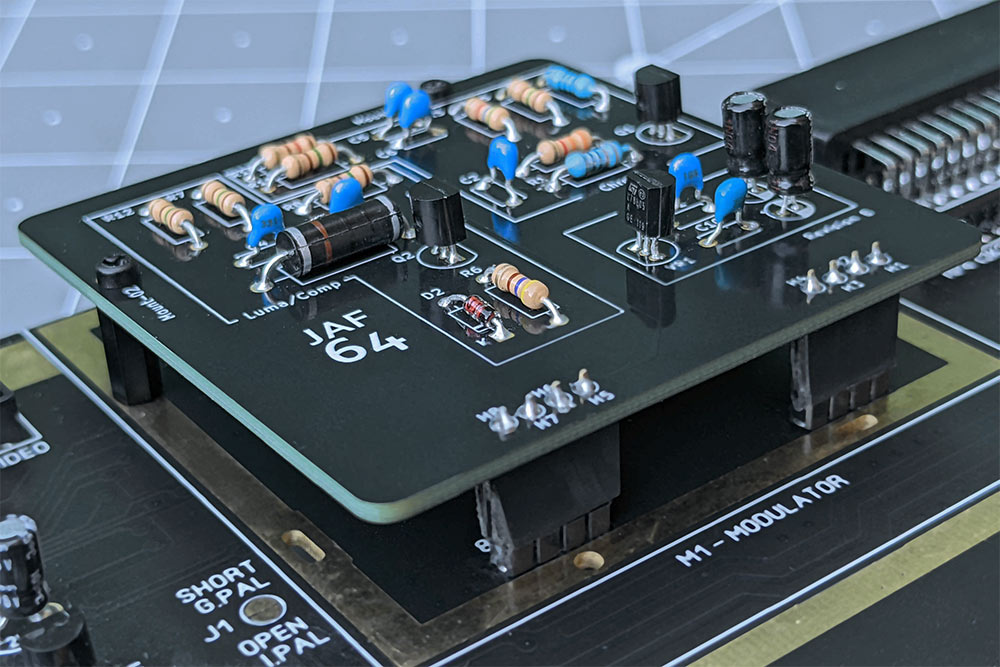
The JAF64 (Revision B) in its completed glory


Although I've still got a lot of experimenting to do, this seems like a good time to reflect on what I've achieved so far.

Despite having high hopes from the outset, I never dreamt I would actually be able to see this through to completion. I fully expected at each stage to hit an insurmountable roadblock so to be holding a kinda-working PCB in my hand is something I'm mighty proud of.

I have obviously learned a lot along the way, but there are still massive gaps in my knowledge and my fundamental ignorance of basic electronics has, without doubt, made things much harder. Instead of making educated decisions I'm guessing and stabbing in the dark which is a long way from ideal. For this reason it's pretty obvious I've got to this stage by pure luck. However, without doing something like this, I'd learn nothing and at the very least I now know what I don't know.

If I have one gripe however, it's that pretty much all of the online explanations I could find for more complex things, like how transistors work for example, are utterly impenetrable for a novice (once you get passed the basics) and believe me, I've tried: VCE, IEQ (amongst a plethora of other things)? Nope, not even the faintest whiff of a clue what they mean, why they're important, how to apply them or how to calculate them. A common theme is the reader should already have a certain level of knowledge and if you don't? Well tough titty, and that's a shame. I have no idea where to even start learning that stuff.

What is the future for this project?

I've already started to make changes to the design based on my soldering experience (enlarging the solder pads) and I've made some minor changes to the trace routing to eliminate vias and add capacitor C1 back in (see below). I will widen the traces and I want to make the whole circuit more efficient so will cut some trace lengths by shuffling a few components around but overall, because the existing design is, as far as I can see, noise and interference free, I'm not minded to make radical changes.

Obviously I need to get to the bottom of the concerning R1 resistor issue and this will require a great deal of digging, which I've started in earnest: I now know R1 provides the base of the transistor with a reference to ground, and I know that the lower the value of R1, the lower the impedance of the chroma signal to ground. In other words: higher resistance (e.g. 1K Ohms) allows less signal to ground, forces more signal to the transistor and thus increases gain - thats high impedance. Lower resistance (e.g. 360 Ohms) allows more signal to ground and less signal to the transistor, lowering gain. Thats low impedance. Oh and now I also know that when using the word "impedance" we are referring to resistance but on Alternating Current, so the Chroma and Luma signals coming out of the VIC-II are AC, not DC. Even that wasn't obvious to me, coz I've never studied electronics, but when you realise that, it becomes clear why the capacitors in the chroma line are important, to filter out unwanted DC signal (see below about Capacitor C1).

However, none of this tells me why lowering the impedance, which is what I've done, makes my circuit work in the PCB but is not required in the breadboard with identical components. I've clearly messed something up but I'm not seeing it yet. 

Whether all that is related to the picture softness and slightly inaccurate color output remains to be seen. Neither of these issues are that bad (I am being particularly critical for complete honesty) and so I want to undertake some burn in tests and just run the thing for hours to test robustness.

I've also discovered that removing capacitor C1 was a mistake. If you cast your mind back to Phase 1, Part 5 I removed this from the chroma circuit at the same time as I removed inductor L1. Together these components created a band pass filter to remove both high and low frequencies from the chroma signal but it seems capacitor C1 is still required to ensure only the AC (Alternating Current) part of the chroma signal is amplified by the transistor (coz this is an amplifier that we're building here) as it impedes the low frequency DC element. As such C1, acting as a high pass filter, will categorically make its way back into a future Revision C and I do wonder if its removal, and the consequent increase in unwanted DC to the transistor base is why I've had to reduce the impedance? That kinda makes sense but I keep coming back to "it freakin works on the breadboard!" Who knew capacitors did so much? Not me that's for sure.

In other words, I'll keep plugging away at my design and try to comprehensively answer the questions and concerns still hanging over it. I will eventually write an update when I've resolved all this. [Edit: It's resolved and that write up is here]

I'm definitely within spitting distance of achieving what I set out to do and designing a working modulator from scratch. For me, that's pretty damn epic.

Please note, it's not my intention to make this design publicly available yet. I couldn't, in good conscience, release a design I don't fully understand, and as there are already plenty of well thought out and effective alternatives out there, if you are in need of an RF Modulator replacement I would politely direct you to them.

If I manage to resolve the issues and concerns outlined above I may consider releasing as a Shared Project on PCBWay though in all honesty I truly see no need: this was always a personal project simply for learning, the fun of it, and the satisfaction of actually making something from scratch.


Costing Up

Creating this PCB wasn't free of course, and I like to keep a record of my spending, both as a personal reference and to give others an idea of exactly the sort of investment they are looking at when embarking on these types of projects. Bear in mind these costs are only accurate now (June 2022) and will become less indicative as time moves on. I also ordered way more components than I needed for a single build so I could experiment - that pushes the cost up too. Future revisions will only add to this. All that said, below are the full details of my spending for this project now. All costs include delivery where applicable, and do not include items I already had (solder, Dupont wires etc) but which were still necessary for the project.

TOTAL PROJECT COST:

R&D Costs

£4.99     -  9v Battery Snap Connectors (Amazon)

£9.99     -  3 x Breadboards (Amazon)

£21.25   -  4 x Transistors (Ebay - a total rip off)

£43.39   -  Revision A Components (Digikey)

£31.55   -  Revision B Components - Voltage Regulator etc (Digikey)

£2.58     -  20 x Resistors (Ebay)

£113.75 -  Subtotal

Manufacturing Costs

£75.23   - Revision B PCB Manufacturing (PCBWay)

Total Cost

£188.98 GBP (€220.04 EUR, $231.94 USD)


I also invested a great deal of time over the 50 day development period. My best guess to that is approximately 100 hours including learning KiCad, creating all the graphics and writing up this blog. I think this was time and money well spent to fulfil this particular ambition, but I understand if many don't agree - one can, literally, go and buy an excellent C64 Modulator replacement for less than £15. For me, that wasn't the point and I really do have a tremendous sense of achievement about the whole experience. That's no bad thing. That's no bad thing at all.


Designing a C64 RF Modulator Replacement Phase 2, Part 2

Designing the PCB in KiCad

In Phase 2, Part 1, after much graft, I got the hang of designing my modulator replacement schematic in KiCad. Now I am ready to take all the parts I have specified in the schematic, and import them into KiCad's "PCB Editor" to begin to layout the actual printed circuit board (PCB) I want to have built.

This is both daunting, and exciting. Daunting because, as with pretty much everything I've done so far I'm still winging it. Exciting because this is the stage an actual working PCB might actually start to see the light of day.

I'll say right upfront what I found most difficult about laying out an actual PCB was moving my thinking away from the breadboard design. In retrospect I actually found laying out my prototype breadboard extremely easy as the physical limitations of a breadboard force you to create a logical "chain" of components. It was something of a struggle to apply some lateral thinking to what I was doing and modify the layout to favour a circuit board. However, this is my first ever attempt at doing anything like this and if I can produce something which works, I'll consider that a triumph. I can always worry about a better layout later.

Before diving into the software, I had a few initial thoughts from the outset that will determine how I progress.

Firstly, I knew that I wanted my PCB to utilise ALL of the available space on my SixtyClone board:


As you can plainly see, outlined in red there is a blank area on the SixtyClone PCB which is approximately 6cm x 6cm specifically for an RF Modulator. It made sense to use all of this available space. Nothing else is going here so why wouldn't I?

Secondly, I wanted to keep all of my different circuits (Chroma, Luma/Comp, Power) as physically far apart as I possibly could to prevent the signals from leaking into each other and introducing interference or cross-talk (defined as: undesirable signals from a neighbouring transmission circuit). With this in mind, I knew from the outset I wanted a 4 layer PCB. One layer would be used predominantly by the Power Circuit, one for Chroma, one for Luma/Comp and the fourth for Ground. In my brain this allows me to keep them all physically separate both vertically and horizontally, though I'm well aware that because energy and electromagnetic fields travel along the path of the circuit and are not actually in the copper per se that this is far more complicated than it seems and my thinking is probably naïve. This is all very "suck it and see" and there's a lot I simply don't understand. The big question I suppose is "do I understand enough to pull this off?" We're already well beyond anything I thought possible so let's bash on with guileless enthusiasm.

Ok. I know I want my PCB design to fit inside an approximately 6x6cm square. I also know that I must have 8 connection holes in the PCB to accept my 7 input and output signals (I'll also have a hole for the audio signal but that won't be connected to anything). I also know that these 8 holes will basically be a fixed reference point within my 6x6cm design. They need to be in a fixed position to allow connection to the SixtyClone board so they cannot move. I also know I can't simply have my PCB supported by the 8 power and signal pins alone, it's far too big for that, so I'm going to have to incorporate some means to physically support my PCB onto the SixtyClone AND I want it to be able remove the board so it can't be soldered directly to the SixtyClone. I have some ideas but first I need to get some more precise dimensions than my 6x6cm approximation. For that it's back to the Service Manual which, on Page 26, provides layout and dimensions for the RF Modulator:


This is a really bad scan (and, unfortunately, the only one I have) so the first thing I did was create a cleaner copy:


Now far be it from me to criticise anyone else, and this is probably just me being stupid, but I found this far more confusing than helpful. Let's break it down:

I can clearly see the 8 holes in the board, labelled 1 to 8 for my power and signal pins and I can also clearly see that the gap between pins 4 and 5 is 24mm. This is good and gives me the first dimension I need. If we then suppose that I want the middle of my board to be halfway between these, then the middle of my board is 12mm between them. So far so good - this would be the red vertical line in the above diagram. What this schematic doesn't give me is the outside dimensions of the original RF Modulator PCB. The 60.8mm measurement is between the pins of the metal shield surrounding the modulator PCB but we can easily surmise that the original modulator is within that.

For my board, I want to utilize two of the locations for these pins as locations for holes to support my board on the SixtyClone. My idea is to use 10mm M2 standoffs bolted to the existing holes on the SixtyClone so I want the exact positions of the circular hole at the bottom right of the above diagram and the circular hole at the bottom left (I'm not interested in the oval shaped holes) relative to the fixed position of the 8 input/output holes. Given the information available in this schematic I'm not entirely certain I can do that. At no stage is it explicitly stated that the middle horizontal line is in fact, in the middle - I have to assume it is. In the following diagram I've entered dimensions I can extrapolate; question marked those I can't without assumption; and in purple, measurements which when I extrapolate further make no sense and are contradictory:


Example: if, from the vertical centre line it is 12mm to the middle of connector 5 and connector 6 is another 2.5mm as specified in the original schematic, that means the distance from the centre line to the middle of connector 6 must be 14.5mm. It must then hold that the distance from the centre line to connector 3 must also be 14.5mm which means the total distance from middle of connector 3 to middle of connector 6 is 29mm. Now in the original schematic it's very hard to make out but I think it says 29.4 (possibly 28.4) neither of which make any sense and that's kind of crucial to know because I need the distance between holes "J" and "I" which could be 29mm or 29.4mm?

For clarity it's the holes I've labelled "F" and "I" in the above diagram I'm trying to precisely locate because these are where I want to mount my PCB. Maybe I've just had a failure of logic but I'm just not seeing how I can do that with the dimensions Commodore provided without making assumptions, other than hole "I" which I can extrapolate as 57.4 mm from connector hole 3 (but only if we assume the centre of "B" is in line with the centre of connector 6 which is also in line with the centre of "J"). What a mess. Or maybe I'm just getting hung up on 0.4mm difference which possibly isnt that big a deal. A good schematic shouldn't leave you guessing though.

Add to all that, the signal and power connectors I'll be using are 2.54mm apart and NOT the 2.5 indicated in the schematic, in the end I pretty much abandoned trying to get this to work and went with the brute force option of taking the actual RF Modulator I removed from my breadbin C64 and punching the pins through a "post-it" note and measuring the distance between them. I figured this was just easier and probably just as accurate.


I suppose we'll see if this was successful if I'm ever holding the PCB I'm designing in my hand!

Now that I know how I'm going to position the 8 input/output holes and the two holes for securing my PCB to the board, I can create a PCB outline in the PCB Editor with these elements as fixed locations and then build the rest of my circuits within these boundaries:


I won't pretend it didn't take me a while to work out how to do this relatively simple process (especially the curved corners), but by using the ruler tool and user layers to store temporary marks and annotations I was able to position these elements precisely where I think they need to be relative to each other. I hope it now obvious why I wanted to pin these measurements down as it's now perfectly clear the area within which I can build my circuits.

My design measures 63.6 x 64mm and is slightly off centre - a vertical line between the 8 holes is NOT the centre of the board - rather there is 33mm between the left edge of the board and this line, and 30.6mm between this line and the right edge of the board. This is to accommodate the metal cartridge guide which I will be inserting into my board at some point. I think I've accounted for all this correctly. We shall see I guess.

In the above image, I deliberately hid many elements to illustrate the initial setup. In reality, the first thing I did after setting up my board outline was import ALL my components from the Schematic Editor. This is done by pressing the button I've highlighted in red below:


Rather than demonstrate what happens if we do this with all my components which would just be a confusing jumble, allow me to demonstrate what happens if I just import the components for a simple 5v regulator (2 ceramic capacitors, 2 polarised electrolytic capacitors, the voltage regulator and the necessary pin connectors):


On import, KiCad just bunches all your components together and it's up to you to separate and order them. In the image above I've pulled them apart so that you can see the individual parts. You can clearly see there are "wires" connecting the components together and this is KiCad's way of telling you which components need to be connected to each other based on the schematic. The more components you import, the more confusing this "rats nest" of wires will become.

By moving, rotating and generally just being imaginative, below is one way in which to connect the components:


To illustrate my point I've very quickly thrown together an example of how you might arrange these components, and I've used the "route tracks" tool to literally draw my traces (in red) between the parts of the components that need to be connected. As you do this, the rats nest of KiCad's connection wires will disappear because it knows when you have connected components together. Obviously I'm definitely not saying this is the best design, it's just one way that seems both compact and meets all the design rules. For Ground you will see that there are no tracks or wires at all. This is because I've created a "filled zone" on a different layer which to all intents and purposes is just a solid layer of copper which links all the ground points together but leaves the other points alone:


In the above illustration the "filled" ground zone is now visible and looking closely you can see that the component holes which need to be connected to ground are connected to this zone by "spokes". Everything else is isolated from the zone and therefore free to go about its business.

Now clearly I've not covered every single step. Once again I have summarised the whole process massively but this is the general idea: You position your components in such a way as to ensure the traces are as short as possible, whilst still ensuring the electrical rules are followed. It's very much like a puzzle and you need to think logically and laterally to make this as successful as possible. I poured over all of this for days and days until I had a design I was reasonably happy with.

The PCB Editor in KiCad also allows you to see a 3D view of your board. This is extremely helpful in giving you an overview of your progress and I will admit I found using that very satisfying! For the quick example I threw together above the 3D view looks like this:


Obviously you can rotate this any way you like to get a view from any angle.

So with the quick example now explained, it was using these exact same principles that I finally managed to design a PCB for my modulator that I was reasonably happy with:


And there it is. My "JAF64" has finally been turned into a virtual PCB. It has my desired 4 layers, I believe the dimensions are as I need them to be and I've kept all of my circuits as far apart from each other as I can. Now this is not to say it's perfect, it's not, and I've already thought of ways I can change this for an improved Revision C. However, there comes a time when you need to draw a line in the sand and say, "Enough, let's get this thing manufactured and let's just see how it measures up." So that is exactly what I did.

If you've ever watched a YouTube video which has any connection to electronics or retro-computing almost all of them are sponsored by PCBWay. I'll be honest, I have no idea which PCB manufacturers are better than others but being that I knew about PCBWay from being subjected to a bombardment of advertising, and being that I could sort of understand what I needed to do to get this manufactured via their site and given that the initial quote was around what I thought was a fair price I just thought "to hell with it" and went with them.

A page on their site told me how to export Gerber files from KiCad which I did, then uploaded. I selected a 1.6mm thick board, with black solder mask, white silkscreen and an Immersion Gold finish which is what I think will closely match my SixtyClone board. The cost for the minimum order of 5 PCBs and postage to my home in Scotland was $88.82 USD. Total cost per board then is $17.76 (or $11.94 excluding postage). Below is a screengrab of the total progress of my order so you can see the timescales and steps involved:


Now we wait for a delivery from Shenzen and we'll cover what happens when it arrives in the next, and penultimate part of this series.


Designing a C64 RF Modulator Replacement Phase 2, Part 1

Building the Schematic in KiCad

If you've been following along with this series of posts about trying to build an RF Modulator replacement from scratch, you'll know how I got to where I am now. There have been frustrations, confusion, misunderstandings, blind alleys and a memorial service for a Zener Diode. Ultimately though I achieved something approaching a staggering triumph. Some might call it blind luck. Either way, at the end of Phase 1, I had a working prototype which I've dubbed the "Janky as F**k 64" , or JAF64 for short.

The JAF64

Here, at the start of Phase 2, I need to take the design and replicate it in software. The software I selected for this task was KiCad.

It must be said, I cannot possibly give a blow by blow account of everything I had to learn and what you need to know to start designing a PCB. Seriously. This series would never end! And we do need this series to end at somepoint.

So with that said, what follows is a heavily abbreviated summary of my experience with KiCad.

On first opening the software (I'm using V6.0) you will be presented with the following interface:


KiCad is a suite of individual elements that work together to help bring your project to completion. The first thing you need to do is create a new project. In the screenshot above I've created a project called "Example" and it has automatically created two files: "Example.kicad_pcb" and "Example.kicad_sch". These are the two elements you will be using 99% of the time.

In the "...kicad_sch", the Schematics Editor, it will come as no surprise that you need to construct your schematic, and once that's complete, you use the "...kicad_pcb" the PCB Editor, to import all the parts and connections you specified in the schematic, to construct a virtual PCB.

So, the first thing that needs to be done is to start building the schematic. Simply double click the "...kicad_sch" element and a blank schematic will open:


This is the blank canvas on which the schematic needs to be drawn. There are a bunch of menu options and icons which can seem pretty overwhelming at first but most of the time I found myself only really using a couple. Most importantly, you need to be able to place components. To do this you need to find "Add Symbol" in amongst the icons or menus:


I found myself accessing it through the "Place" menu most of the time but there is also an icon to the right which will do the same thing. As will pressing "A" on the keyboard. Either way, a new window will open:


This is where things get messy. You need to find the symbol for the component you need from amongst a list of over 17,000 symbols and it isn't particularly obvious. Say for example I know I want to insert a capacitor:


I narrow down my search by starting to type the word "capacitor" in the filter text box at the top of the window. After I had typed "capa" the available items had diminished somewhat and I can start to see item names like "D_Capacitance" and "C_small" and so on. If I'm looking for a symbol for a regular unpolarised ceramic capacitor, then at least one appropriate symbol is found by selecting the item "C", as pictured, C being the universal designation for a capacitor in a schematic I guess? With "C" selected, and the symbol that I want presented, I press OK.


This brings me back to my blank template where I can just use the pointer to drop the symbol wherever I want it. The next thing that must be done is to give this capacitor a unique reference number, and we must tell the software the value of the capacitor (i.e. it's capacitance). You can't omit this or KiCad throws a hissy fit later.

By right clicking anywhere on the symbol, a menu will appear:


From the menu, select "Properties..." as shown.


The Properties window will open. Beside "Reference" type the unique reference you want to give your symbol (in this case I used "C1") and beside "Value" enter the capacitor value, which in this case I've entered "4.7μF". Then press OK.


The symbol is now labelled. If I want to rotate the symbol, I simply press "R" and it will rotate 90 degrees:


The final thing that MUST be done with this symbol is to assign a footprint. This is an absolute pain in the arse but there's no getting away from it, KiCad needs to know the physical dimensions of the part so we know how much space it will take up on the PCB afterall.


Once again, right click on the symbol and this time select "Edit Footprint" (or press "F"). A new window will open:


If there is already a footprint assigned to the symbol, you will see a designation entered beside "Footprint", but in this case it's blank so we need to find a suitable footprint in the library. Press the button that looks like 3 books to the right of the window and another window will open:


And once again we are required to search through a list of thousands of footprints to find something suitable:


Here, at the top left, I started to search for "capacitor" and the available options diminished. I know I want a "through hole" capacitor so the abbreviation for that is THT (as opposed to a surface mount capacitor which has an abbreviation of SMD for example). So I select Capacitor_THT on the left, and to the right of that I am then presented with a long list of available footprints for through hole capacitors of all varieties. Here it's simply a case of finding the most suitable footprint based on the type and dimensions of the capacitor in question. In this case I decided that the footprint for a ceramic disc capacitor with 5mm pitch (distance between component legs) would be the best so I selected that and a picture of the footprint appears in the main window. You will need the datasheets for every component handy so you have some idea of the footprint you need.

To assign the footprint to the symbol press the button that looks like a chip with a red upward pointing arrow (highlighted):


You will then be returned to the initial "Edit Footprint" window which is now populated with the footprint you selected:


Press OK and you will be returned to your schematic. Nothing obvious will have changed but you have now done everything necessary to ensure that component will export correctly to the PCB building element.

You then need to repeat that whole process for every single element on your schematic. You will age drastically doing this, though in fairness all the capacitors I used in the end had the same footprint so I was able to simply copy and paste the initial symbol and only needed to change the reference and value. The same was true with the resistors.

Obviously you need to "wire" your components together and as well as being in the "Place" menu, you can access the Wire icon in the menu to the right:


Pressing this will allow you to click on a node of your component and start adding a wire to it:


Here in this simple example you can see I've added a wire to the right node of my capacitor and started drawing it to the right. And that's pretty much the jist of it. You add components, rotate and position them, apply unique references and values, add the appropriate footprint, wire them together and repeat over and over again until the job is done. It took me flippin hours to do my extremely modest schematic but we got there in the end with a lot of help from YouTube:

Click for a much larger image

By far the most complicated part was working out how to correctly tell KiCad I was bringing the power and signals into the board from an external source and exporting those signal to an external source (that external source being the 250466 C64 PCB) but I did work it out eventually thanks to YouTube.

As I've said, I have summarised but the above is enough info to get anyone started and there are enough tutorials online to answer all questions that might crop up. That's how I got through it anyway and if I can do it, anyone can.

The final step before progressing to the PCB design is to perform an Electrical Rules Check. Press the button along the top of the screen that looks like a checklist with a red checkmark. This is really important to ensure you haven't messed up.


You are aiming to have no Errors and no warnings.

As I said, for me this took a long time to get right but I did eventually get there. In Phase 2 Part 2 we will import the components I specified in this schematic into the PCB designer and get the creative juices flowing.


Designing a C64 RF Modulator Replacement Phase 1, Part 5

Prototyping with a Breadboard

Revision B

Lets start, as always, with a recap. I had this zany idea to build my own RF Modulator replacement for my SixtyClone C64. In Part 1 I gave my reasons. In Part 2 I messed about with the original schematic to come up with my design. In Part 3 I tracked down my components and in Part 4 I built Revision A on a breadboard and failed to get it to work, blowing a Zener Diode in the process and nearly burning up my transistors. I decided my power circuit was hopeless and researched a new and simpler design.  You should probably read all that first or much of this won't make sense.

Anyway, this brings us up to date. This initial failure will come as no surprise to anyone. I have been totally winging this whole endeavour and have virtually no clue what I'm doing. It's kinda fun though, which is sorta the point.

The new components required for my simpler power circuit arrived a few days after ordering. I laid out my breadboard according to the voltage regulator's datasheet and added 10μF electrolytic capacitors as follows:


With my 9v battery attached to this circuit it was outputting 5.02 volts which was exactly what I was hoping for. Because I'm new to this, it's still a pleasant surprise when a component behaves the way it's supposed to!

I then decided to take a look at how diode D1 was going to affect the voltage to the rest of the board. All I know about Diodes is they allow current in one direction and prevent current from travelling in the other but how does this affect voltage? More specifically, do they lower the voltage in the direction current is allowed? Only one way to find out. Test it.

With the diode in circuit my output voltage reading was 4.66 volts. So yes, the diode was costing me 0.36 volts. Do I need to be worried about that? The answer to this, like many other questions, was not forthcoming but I decided to remove it for initial testing and see what happened.

Once again, it was with great trepidation I wired my rats nest breadboard to my SixtyClone and switched on.


Holy shit. It freakin' worked!!!

I absolutely did not expect that. Seriously. And this time, no burning smells, no over heating, just a steady, sharp and colorful screen. I wish I could express in words just how good that felt.

Yes, ladies and gentlemen, I am proud to announce that I did indeed blunder my way to building a working prototype of a C64 RF Modulator replacement on a breadboard. And writing this a whole 48 hours after the event, I still can't quite believe I managed it.

Prototype - Revision A

After the initial wave of shock and amazement passed, I was able to pass a more critical eye over what I was actually seeing over a solid hour or so of testing:

The Good

Colors were nicely saturated and accurate
Text was sharp with very little color smearing.
Only the voltage regulator got warm and never too hot to touch.

The Bad

Touching some of the wires on my breadboard caused interference and interruptions to the video signal which meant the physical connections were crap.

The Ugly

It was a very, very noisy picture. This doesn't come out in pictures at all so you're just going to have to take my word for it, but the best way I can describe it is like a layer of colourful static with a slight magenta hue overlaying everything. This static was also swimming slightly.

Some Experimentation

So, obviously the first thing I can say with certainty is that diode D1 is not required. I didn't feel the need to put it back.

Next thing I did was re-seat some of my wires. I also reduced the length of the "luma out" wire which was causing the most interference when I touched it and this definitely helped reduce the interruptions to the signal at the expense of making the wire tighter than I would like. It did reduce the noise however.

I then had a think about the chroma signal. I know from my social media intake that the s-video output from a C64 isn't standard and many people who build their own cables (and I've watched them do it on YouTube) incorporate a resistor into the chroma line. I have not built my own s-video cable, and have no idea if such resistor is present in the one I bought, and I'm not about to take it apart to find out either. In the advertising blurb of the cable however, it does state "has modifications to improve picture quality and reduce audio hum" which probably means it does. What I know for certain is that in my chroma circuit, the final resistor in the chain before the signal leaves the board and heads to the cable is R4 and is 180 ohm, as specified in the schematic. I wanted to see what happened if I changed the value of this resistor.

I removed the 180 ohm resistor and replaced it with a 330 ohm resistor. This categorically made the picture worse and emphasised the existing noise. I removed that and inserted a 100 ohm resistor. That categorically improved the picture and whilst the noise was still very much present, it stopped swimming and was definitely cleaner, or at least de-emphasised.

I did the same with the last resistor on the luma circuit, R7, and at 330 ohm it started to lose sync and the picture started to scroll. No bueno. Back went the original 150 ohm resistor

During my research I came across this video by Adrian Black. The whole video was fascinating: not only his revelation that there are far more revisions of C64 RF Modulator in the wild than the two schematics in the Service Manual would suggest, but also his honing in on the need for the inductor (L1) in the chroma circuit. The message in that video was unequivocal - it is not needed and its existence in the circuit actually causes blurring in the video output. He also demonstrated that L1 was not present in PAL versions of the modulator, only in NTSC versions. Why on earth would this be?

The eminently sensible and easy to follow answer was actually in a comment by Craig Sherman under the video: it was put there to meet strict FCC requirements and was done "to help reduce dot patterns when watching the RF output on a B/W TV and to eliminate adjacent channel interference... By eliminating the choke [another term for inductor] you are allowing the chroma signal to have as much 'sharpness' as the luma."

I love it when a technical question comes along and is answered in plain English that makes perfect sense. As a result I doffed my cap to those with far more knowledge than me and I simply removed inductor L1 from my build. This also meant, I supposed, that I could remove capacitor C1 from the build too: an inductor and capacitor together like this in a circuit is called a "Band Pass Filter": the inductor impedes high level frequencies from the circuit; the capacitor impedes low level frequencies. This leaves the mid level frequencies to get through. But as we are removing one I figured the other isn't required either. So I waved bye bye to C1. Removing these in my breadboard definitely cleaned things up a bit, though I can't say my picture was blurry in the first place. What I categorically did notice was a reduction of color noise throughout, leaving just a plain static noise overlaying the picture.

I also experimented by removing capacitor C6. This has the effect of disconnecting the chroma circuit from the composite circuit, which would mean the composite signal would just be black and white - not really a problem as I'm only using the luma and chroma circuits for s-video output. I wanted to do this however, to determine if this connection was somehow feeding back into the luma circuit and creating unwanted noise. In either case it didn't matter, removing it made no difference and given that if I ever wanted to use composite I'd rather it was color, C6 stays in.

This leaves my schematic looking like this:


Nothing I did above completely eliminated the ever present "static" noise I was encountering though. Now, whilst this noise was far from ideal, I do have to put on record that I could easily live with it if necessary - the video out from my janky as f*** breadboard was by now actually remarkably good all things considered and the noise I'm complaining about isn't visible during fast moving demos for example, only on solid colours.

I then wondered if breadboards are inherently "noisy" themselves? It strikes me that flippin' great tangles of cheap wire with tenuous connections literally hanging out all over the place couldn't possibly be good for a sensitive TV signal? I Googled it and very quickly came across this forum post from where I found the following piece of wisdom, posted by AndyC_774:

 "I dislike breadboards, and stripboard isn't much better. Both are good ways to hook a few parts together quickly to check that they work more or less as expected, in a very rough & ready way. Once you start looking for accuracy, quietness and precision, they very rapidly become your worst enemy"

Now this is very obviously confirmation bias, but I really do believe, at this stage, that the "static" noise I'm seeing is because of the breadboard and not the design. All my decoupling capacitors are in place as specified and no amount of tinkering on my part improved things any further. I could however, easily be wrong, I frequently am, but I don't think I can address the noise issue any further without taking the breadboard out of the equation.

I can scarcely believe it myself but I actually think my prototype, and with it Phase 1 of this project is complete.

Janky As F**K (JAF)


So. It's time to move on from the breadboard, and actually design a PCB. Holy shit. I never, ever thought I'd get to say that!

Queue hours and hours of Googling and YouTube watching.

After a great deal of this I decided the software I was going to use to design my PCB was KiCad because it comes very highly recommended, there are plenty of tutorials on YouTube, and it's open source which is important because I really don't want this project to necessitate a mortgage. That aside, I'm under no illusions. This is going to be a real steep learning curve (have I mentioned I've never done anything like this before?) and I do not doubt this will be something of an ordeal!

In the next entry, I will let you know how I get on.

Before closing I confess to being a bit ill at ease with my existing transistors at Q1 and Q2 (2SC1684T). Not because they don't work - they actually seem to work perfectly - but rather because the only place I could get them was bloody Ebay and at a hugely over inflated price (£5 each!) so I'm going to research different transistors that I can easily obtain from Digikey at a much more sensible outlay.


Popular Posts